This thread has been locked.

If you have a related question, please click the "Ask a related question" button in the top right corner. The newly created question will be automatically linked to this question.

ADC12DJ5200RF: Power Supply query

Part Number: ADC12DJ5200RF
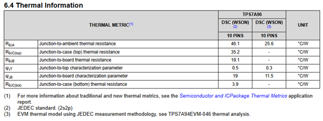
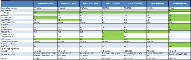
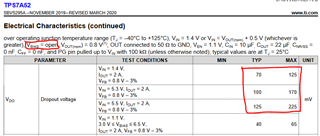
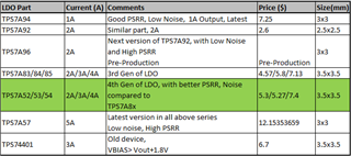
Other Parts Discussed in Thread: TPS62913, , TPS7A94, TPS7A92, TPS7A96, TPS74401, TPS7A84A, TPS7A52, TPS7A57, TPS7A54

Hi Team,

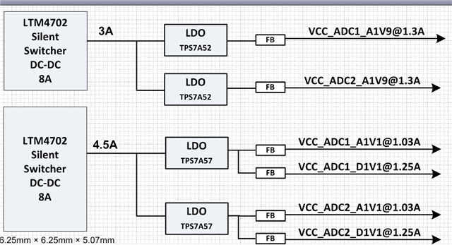
We are using 2 ADC12DJ5200 for 4 Channel 

I've few questions on power supply regulator + LDO vs Silent switch  TPS62913

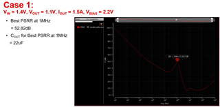
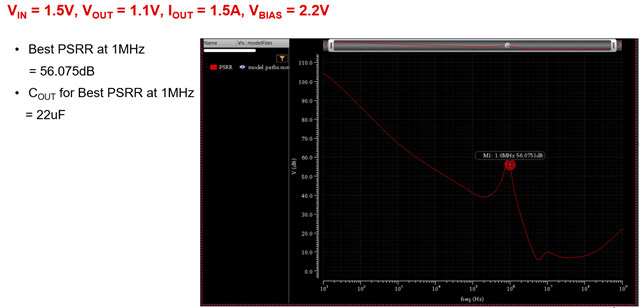
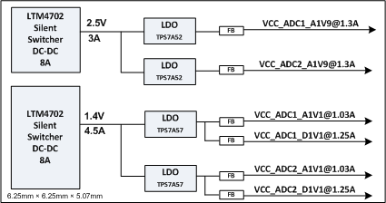
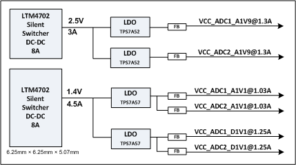
Case1: Using Regulator + LDO,

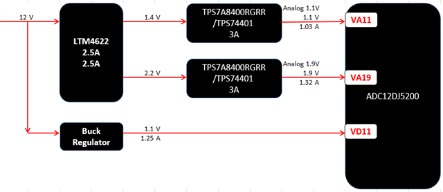
Q1: Can the Digital 1.1V (VD11) Supply be directly sourced from Switching regulator or Should be from LDO?

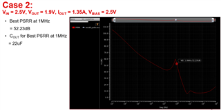
Case2: Using Silent Switcher: TPS62913

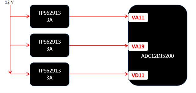
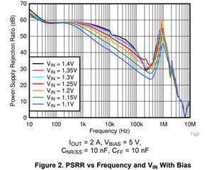
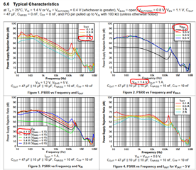
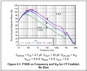
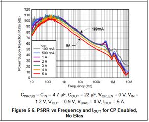
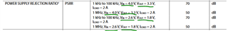
Q2: For the silent switcher IC, Can you please share the PSRR values?

Q3: Which one do you suggest over Case1 vs Case2?

Q4: Related SPI Signals of ADC12DJ5200, Control signals are referenced to 1.9V(max), Can I directly connect the SPI signals to controller (Xilinx FPGA) 1.8 Level support? Or recommends level translator?

Thanks.

  • Hi Team,

    Awaiting for your response

  • Hi Lakshminarayana,

    1. VD11 can be directly supplied from switcher. 

    2. Here is the PSRR data for the ADC12DJ5200RF. 

    2. PSRR DATA -.xlsx

    3. Case 1 should yield better performance. 

    4. USE a level translator. 

    Regards,

    Neeraj

  • Hi Neeraj Gill

    Thanks for your information.

    PSRR data of silent switcher seems to be lot lesser when compared to LDO. (which is different from mentioned here  Powering Sensitive ADC Design with TPS62913

    We will use the silent switch for Digital Supply and For Analog supply we will use combination of Switching regulator with LDO for better performance. Is this Okay?

    Does SPI, IO's requires level translator? We thought FPGA IO will be 1V8 and ADC IO will be 1V9.. we thought, we can directly connect

  • Hello, 

    The PSRR data provided by Neeraj was for the ADC, not the TPS62913. The TPS62913 PSRR data for differen input/output combinations is shown in the TPS62913 datasheet (see figures 6-45 through 6-48). As you can see in the application note, the performance of the ADC is not degraded when you use the TPS62913 without an LDO for all the ADC rails and the clock power supply as well.  

  • Hello  / Neeraj Gill

    Does SPI, IO's requires level translator? We thought FPGA IO will be 1V8 and ADC IO will be 1V9.. we thought, we can directly connect

    Can you also update on SPI IO Level query which i asked previously?

    Also, Your feedback on this: 

    We will use the silent switch for Digital Supply and For Analog supply we will use combination of Switching regulator with LDO for better performance. Is this Okay?

    Thanks

  • Using an LDO after the TPS62913 is a good approach if needed.  We have an app note in work showing that you can use a low noise converter like the TPS62913 and an ultra low noise LDO like the TPS7A94 and get the same noise performance with a lower LDO dropout, hence saving power.  It should be published shortly.

  • Sure

    Thanks.

    TPS7A94 is a 1A Part, Do you recommend any same series 2A part with good PSRR?

    For the ADC12DJ Digital supply can be directly from switcher. Is my understanding correct?

  • Hello, 

    The TPS7A92 is a 2A LDO with 4uVrms noise. All rails can be supplied directly from the TPS62913 with no issues, as shown in the app note you referred to earlier. 

  • Hi Steve Schnier / Neeraj Gill

    We have Two ADC12DJ5200 in our design.

    Do you recommend using two separate LDO's for each ADC's or We can combine the common supplies for Two ADC12DJ?

    Thanks

  • Hi Lakshminarayana,

    if crosstalk between two ADCs is not a concern, the same LDOs can be shared. but i would still separate the two ADCs with ferrite bead or three terminal capacitor to get good isolation between them.

    Regards,

    Neeraj

  • Hi  /  Steve Schnier 

    I've concluded to use silent switcher TPS62913 for Digital Supply.

    • Since I've two ADC, Can I combine the digital supply with a single TPS62913 OR Recommend to use separate?

    Regarding Analog Supply,

    • Can I go with this part: ADM7172 OR ADP1763 which seems to have better PSRR than TPS7A92 ?
  • Hi Lakshminarayana,

    Two TPS62913 are always better on the digital supply.

    Steve, will need to comment on the TPS vs. the ADP/ADM devices. I can only say is the PSRR really needed?

    Do you have a noise requirement for the power supply stage upstream before this device?

    Regards,

    Rob

  • Hi 

    • Since we've constraints on board space, I was planning to combine 2 ADC's Digital Supplies using a single TPS62913.

    I can only say is the PSRR really needed?

    Do you have a noise requirement for the power supply stage upstream before this device?

    • There is no such requirement. We have always used high PSRR LDO's to make sure that Power supply noise is not coupled on to ADC Data.
    • In previous RFSoC based projects, we have faced issue with Low PSRR LDO's.
    • One more question, How is the Internal Power architecture of ADC12DJ5200, Does ADC Chip has LDO's & Filter for Analog and Digital supplies?

    Hi  /  Steve Schnier 

    Can you please comment on TPS vs ADP/ADM devices?

    Thanks.

  • Hi KLN,

    It looks like the ADC12DJ5200RF is a high speed ADC.  For high speed ADC's TI recommends good PSRR in any low noise LDOs that are powering them, as noise can affect the ADC signal to noise ratio (SNR).

    The TPS7A96 is the 2A version of the TPS7A94 but with the same ultra low noise, high PSRR specifications.  The TPS7A96 has 0.46 uVrms noise from 10 Hz to 100kHz and this does not change with voltage because the TPS7A94 and TPS7A96 operate in unity gain feedback.  From the datasheet, the ADM7172 has 6 uVrms which is significantly higher than the TI devices.  The ADP1763 has even higher noise than the ADM7172 and it also increases as Vout increases (see figure 18 in the ADP datasheet). 

    The TPS7A96 has excellent PSRR across frequency that is hard to beat in a low noise device.  From the TPS7A96 datasheet:

    The ADM7172 has about half of this PSRR at low to mid-band frequencies (thus, you need approximately 2 series ADM7172 to equal the PSRR of one single TPS7A94 or TPS7A96 at low to midband frequencies): Figures 32-36 in the ADM datasheet show a flat 50-60dB of PSRR up to higher frequencies. The ADP1763 has worse PSRR at higher load currents (figures 20-22 in the ADP datasheet).  The datasheet comparisons show that the TPS7A96 has the best PSRR of the 3 LDO's especially at higher loads.

    The TPS7A96 EVM is available and preproduction TPS7A96 LDOs can be ordered from TI.com.  Formal production of the TPS7A96 LDOs are expected to begin in the next few weeks.  For even higher load currents than 2A, you can easily parallel the TPS7A96.  In addition to increased load current, paralleling the TPS7A96 has 2 more added benefits you may want: (1) increased PSRR for the same load current, and (2) lower LDO system noise (placing LDO's in parallel reduce the overall noise by the square root of the number in parallel.  Thus, 4 parallel LDOs will reduce the 0.46uVrms in half, etc).  Let me know if you have any additional questions on LDOs.

    Thanks,

    Stephen

  • Hi  

    Thanks for your detailed response.

    ormal production of the TPS7A96 LDOs are expected to begin in the next few weeks
    • Can we order the TPS7A96 LDO's directly from TI? When will it be available at Distributors like Mouser or Digikey?
    • Can we go ahead considering this TPS7A96  part? Since it is a pre-production.
    • What will be the cost for the TPS7A96 

    Another option, we are thinking is TPS74401RGWRG4,

    Can you please compare this TPS74401 and TPS7A96 

    Can you give more info on data

    Also, Please check our calculation of PSRR

     PSRR DATA -ADC12DJ5200.xlsx

    Thanks

  • Hi KLN,

    I'm working on getting the information to the questions in your bullets and I'll hopefully reply back later today or tomorrow with answers.

    I'll defer to Neeraj to comment on his ADC PSRR data.  However, using common online calculators I get the same answer when I take the "Output Ripple" value and calculate the "input power (dBm)" so I think that step is correct.  And your step of adding the PSRR (in dB) for the LDO and ADC together is correct (PSRR of devices in series just add together).  Calculating LDO PSRR can be found in this document and you will want to modify the equation in the "PSRR Data - ADC12DJ5200.xlsx" accordingly:

    Here is a comparison between the TPS7A96 and TPS74401.  The TPS7A96 delivers significantly better noise and PSRR performance than the TPS74401.  While the TPS74401 was a low noise LDO when it was designed 20 years ago, in modern terms it is not really low noise.  The TPS74401 does not operate in unity gain feedback which means that as Vout goes up, so does its baseline 16 uVrms noise by the same amount. 

    • The TPS74401 comes in multiple packages but all are larger than the TPS7A96. 
    • The TPS74401 has worse PSRR and noise performance than the TPS7A96
    • The physically larger TPS74401 also has a larger thermal pad, so you will get slightly better JEDEC thermal resistance with the TPS74401 (around 8 C/W better). Having said that, actual PCB thermal resistance is highly dependent on your PCB layout and in the end both options could be practically the same.  I don't see this as a determining factor in your application.

    Thanks,

    Stephen

  • Hi   and 

    Thanks for your response.

    I think you've forgot to answer for this:

    • Can we order the TPS7A96 LDO's directly from TI? When will it be available at Distributors like Mouser or Digikey?
    • Can we go ahead considering this TPS7A96  part? Since it is a pre-production.
    • What will be the cost for the TPS7A96 

    Please confirm for above queries. 

  • Hi KLN,

    The preproduction LDO's you see available for order right now are the final silicon devices going into production.  So you can order them now for evaluation and the production LDO's will deliver the same performance.

    The TPS7A96 is being released in early August, but possibly as early as the end of this month.  Please check TI.com for when the production units are available, it shouldn't be much longer from now.

    The 1k price will be $3.90.

    Thanks,

    Stephen

  • Hi 

    Thanks for your response.

    We do observe that TPS7A96  is Minimum input voltage is 1.9V.

    We have a case where Analog 1.1V rail to be generated from 1.4V. This TPS7A96  can not be used for that.

    Also, Can you compare the ADC12DJ5200 Eval board LDO TPS7A8400RGRR  vs TPS7A96

    Our Voltage requirement are as below,

    • VIN- 2.2V, Vout- 1.9V Analog, 1.35A
    • VIN- 1.4V, Vout-1.1V Analog, 1.5A

    Please suggest us

  • Hi KLN,

    The TPS7A84A is a good device but it is 3rd generation now.

    To give you some history to help with your decision: The TPS7A83/4/5A series was released first.  Next, the TPS7A52/3/4 were released to improve on the TPS7A83/4/5A.  The biggest difference between the 3/4/5A and 2/3/4 suffix of these devices are the current limits: TPS7A83/4/5A = 2A, 3A or 4A (respectively).  The TPS7A52/3/4 = 2A, 3A or 4A (respectively).  Most recently the TPS7A57 was released, improving on all of these devices.  The TPS7A57 = 5A capable.

    The TPS7A94/6 is Texas Instruments lowest noise LDO in industry, and also comes with high PSRR LDO.  The TPS7A57 was designed for high current, ultra fast transient response, and high performance applications where low noise was required.  These are our state of the art LDOs for low voltage applications.

    Note: The TPS7A57 uses ceramic capacitors on the output.  We need to update the table to reflect this.

    Thanks,

    Stephen

  • Hi 

    Our Voltage requirement are as below,

    • VIN- 2.2V, Vout- 1.9V Analog, 1.35A
    • VIN- 1.4V, Vout-1.1V Analog, 1.5A

    Which one do you suggest for our case?

    NOTE: This is for ADC12DJ5200 ADC Chip

  • Hi KLN,

    For best performance:

    VIN = 2.2V, Vout = 1.9V, 1.35A: TPS7A96

    VIN = 1.4V, Vout = 1.1V, 1.5A: TPS7A57

    Thanks,

    Stephen

  • Hi 

    TPS7A57 is 5A Part and which is bit pricey as well. 

    Our requirement is 1.5A max.

    Please can you suggest alternate part?

  • Hi KLN,

    Yes I can.  The TPS7A57 delivers the best performance but if cost is a concern you'll want to look at the TPS7A52. 

    Thanks,

    Stephen

  • Hi 

    Thanks for your quick response.

    TPS7A52 seems to have 20-30dB PSRR at 100KHz frequency range. Is this okay?

    Seems like TPS74401 has better PSRR compared to this.

  • The PSRR at 1MHz is mostly coming from the low impedance of the output capacitor.  This impedance is a function of the effective capacitance, ESR and ESL as well as PCB parasitics.  Thus, placing the output capacitor as close as possible to the LDO and selecting the smallest package size ceramic capacitor will deliver the best PSRR. We can run IC simulations to find the capacitor that gives you the best PSRR at 1 MHz - let me know if that's something you would want us to do.

    Between the TPS74401 and TPS7A52: It's your dropout I'm worried about.  In the power tree I see at the top of the forum thread, it looks like there are 4 rails: 12V, 1.4V, 2.2V and 1.1V.

    TPS7A52 dropout requirement is 100's of mV or less.  You can easily meet this on the 1.1V output with the 1.4V or 2.2V rail.  The TPS74401 is much higher.  You need 1.6V or 1.7V above Vout on Vbias.  So 2.7V or 2.8V, minimum, would need to exist somewhere but I don't see it.  Even a typical analysis looks marginal at best (see below).  I think the TPS7A52 is safer than the TPS74401.

    TPS74401:

    Here is a typical curve of the BIAS dropout for the TPS74401.  This does not include tolerances, which the 2.2V rail in your system will certainly have.  It just looks very marginal to me and risky to use the TPS74401 with the rails you have for a performance application.  But if you think it will give you the performance you need, then certainly you can try it and we'll be here to support you if you need assistance.

    Thanks,

    Stephen

  • Hi 

    Thanks for your detailed response. 

    We will discuss with the team and get back to you on this.

    We can run IC simulations to find the capacitor that gives you the best PSRR at 1 MHz - let me know if that's something you would want us to do.

    Yes please, at 10KHz, 100KHz, and 1MHz.

    Please let us know how you simulate.

    it looks like there are 4 rails: 12V, 1.4V, 2.2V and 1.1V.

    But 1.4 and 2.2V are generated from Switching Buck regulator. Only 1.1 and 1.9V are from LDO's

  • Hi KLN,

    Please confirm you want the simulation for the TPS7A52?

    Yes I assume that 2.2V would be the bias rail for this LDO generating 1.1V.  Also note that as you get closer to the dropout voltage, the PSRR goes away.  At dropout there is no significant PSRR except what little is provided by the parasitics and output capacitor.  In the TPS74401 datasheet PSRR curves the BIAS voltage is 1.8V higher than Vout to give you those typical curves.  Thus, they used approximately 50% higher than the typical dropout value to get plenty of headroom for good PSRR.  So to achieve similar results, typical, you would need 2.9V for a bias rail and probably a little higher when factoring in tolerances.  The TPS7A52 is easier to obtain good PSRR with your existing rails. 

    Thanks,

    Stephen

  • Hi 

    Can we use the TPS7A52 for the both rails 1V9 and 1V1.

    So TPS7A96 will be replaced by TPS7A52, i.e. Two TPS7A52

    Also, The PSRR Values mentioned in TPS7A52 LDO has a dropout of 400mV, In our case, Drop-out voltage is 300mV,

    Can you please share us PSRR values with respect to Dropout voltage

    Please confirm you want the simulation for the TPS7A52?

    Yes, We want the simulation results for our requirement

    Thanks

  • Hi KLN,

    TPS7A52 PSRR Simulations: 1.4Vin, 1.1Vout, 2.2Vbias

    I'll send a request to the IC designers to start a PSRR simulation on the TPS7A52 for the 1.1V rail.  I'll use Vin = 1.4V, Vout = 1.1V and Vbias = 2.2V.  These requests typically take 2 weeks so lets continue our discussion on the 2.2V to 1.9V option in the meantime.

    2.2Vin, 1.9Vout: TPS7A96 PSRR

    The TPS7A96 will probably give you better PSRR than the TPS7A52 at these loads and with just 300mV of headroom.  These plots are not in the TPS7A96 datasheet yet, but they will be, showing the PSRR with different values of headroom and output capacitance.  Don't worry about the 1 MHz value with 300mV of headroom in the first plot - by changing Cout we can raise this (see the second plot).

    2.2Vin, 1.9Vout: TPS7A52 PSRR

    Do you have flexibility over the 2.2V rail?  If it is only meant to be an intermediate buss, and is only powering the LDO, can we increase the 2.2V rail to 2.4V or 2.5V? The TPS7A52 PSRR may not be very high with only 300mV of headroom typical.

    2.2Vin, 1.9Vout: TPS7A57 PSRR

    This may be something where you need to reconsider the TPS7A57 for the 2.2V to 1.9V rail if we cannot raise the 2.2V or you cannot achieve the performance any other way.  The TPS7A57 will definitely give you excellent PSRR at 1 MHz and ultra low noise with only 300mV of headroom.

    Thanks,

    Stephen

  • Thanks 


    2.2Vin, 1.9Vout: TPS7A52 PSRR

    Do you have flexibility over the 2.2V rail? 

    Yes, This is an intermediate supply for the ADC Chip. We will try to increase the voltage

    Also, Can you check this: ADP7158 This seems to have better PSRR.

  • Hi KLN,

    The ADP7158 is characterized with 700mV or 800mV of headroom.  That is a lot!  We need a better direct comparison.

    Below is a PSRR plot from the TPS7A96 datasheet, to try and match the ADP7158 conditions better.  You can see from this TPS7A96 plot that the headroom is 500mV.

    1kHz: TPS7A96 = 95dB, ADP7158 = 62dB
    10kHz: TPS7A96 = 70dB, ADP7158 = 62dB
    100kHz: TPS7A96 = 52dB, ADP7158 = 52dB
    1Meg (this is heavily influenced by Cout): TPS7A96 = 30dB, ADP7158 = 45dB
    --> We can simulate the TPS7A96 and suggest a different value of Cout to achieve higher PSRR at 1MHz.  It may be as simple as 22uF or 47uF instead of 10uF but we can look.  How much do you need?

    If you are using the PSRR to eliminate broadband noise from a source supply, then the TPS7A96 is clearly the better option even without a new Cout.  The total output noise of the LDO will be the summation of the LDO internal noise with the external noise that the LDO is filtering on Vin.  Noise spectral density is the integral of broadband noise across frequency, thus the LDO that attenuates more broadband noise will deliver lower noise density on the output.  The TPS7A96 already starts with significantly lower internal noise than the ADP7158 (0.47uVrms vs 1.6uVrms) and the TPS7A96 has significantly higher PSRR at low to midband frequencies so it will attenuate the Vin noise much more than the ADP7158.  If you want higher PSRR at 1MHz we can find the output capacitor value to get you that.

    Here is the ADP7158 noise specs.  The TPS7A96 is specified as 0.46 uVrms from 10Hz - 100kHz.

    Thanks,

    Stephen

  • Thanks 

    TPS7A96 is yet to be released

    We have almost concluded that we will go with TPS7A52 for both 1V9 and 1V1 . NOTE: headroom will be increased to 500-600mV i.e. 2.4/2.5V and 1.6V for better PSRR 

    This is what we have concluded from above discussion. please check above.

    Thanks.

  • Hi 

    Awaiting for your response.

  • Hey KLN,

    Per your table: The TPS7A96 is the 2A version of the TPS7A94.  I'm unsure where the TPS7A92 fits in with the history of these other devices.  The price that is listed for each LDO appears to be the cost for a single device and possibly for a distributor.  If you go to TI.com you will get cheaper prices than distributors. 

    With the TPS7A52 and 0.6V headroom from Vin to Vout, the PSRR will be slightly less than the black curve in figure 2 within the TPS7A52 datasheet.  I'll add this use case to the simulation request to see what Cout you need for best PSRR at 1 MHz.  I have these conditions: Vout = 1.9V, Vin = 2.5V, Iout = 1.35A.

    Thanks,

    Stephen

  • With the TPS7A52 and 0.6V headroom from Vin to Vout, the PSRR will be slightly less than the black curve in figure 2

    What would you recommend of headroom? with TPS7A52?

    Please suggest us the best possible ways with TPS7A52.

    Thanks

  • Hi KLN,

    Let me see what the simulations show for the PSRR and I'll get back to you.

    Thanks,

    Stephen

  • Hi KLN,

    The best PSRR at 1MHz is with 22uF effective capacitance.

    Thanks,

    Stephen

  • Hi  

    Does it get better with

    • VIN-1.5V and Vout- 1.1V ?

    Can you also ask your team for TPS7A54?

    Thanks. 

  • Hi KLN,

    The TPS7A54 will not provide different results, it is just a higher current version of the TPS7A52 but the rest of the internal circuitry is the same.  I'll ask on the updated conditions and get back to you.

    Thanks,

    Stephen

  • Hi KLN,

    I'm still waiting on the updated TPS7A52 simulation results with your updated conditions.  But I wanted to let you know that the production version of the TPS7A96 has been released and is now available to order. 

    Thanks,

    Stephen

  • Hi KLN,

    Here is the updated simulation for the TPS7A52 per your request.

    Thanks,

    Stephen

  • Hi  

    Thanks for your response.


    Here is the updated simulation for the TPS7A52 per your request.

    May I know with what load and Input capacitance the above simulation was done?

    We have made few changes in 

    We are also considering TPS7A57.

    Can you simulate for TPS7A57?

    Please consider 3A Load for TPS7A57

  • Hi KLN,

    The output capacitance is listed in those snapshots I provided. It turns out that in each case, 22uF was found to offer the best PSRR.  The simulation did not use an input capacitance because it is in parallel with the input supply and AC injection. 

    I will request a simulation to maximize the PSRR for the TPS7A57 at 3A load.  This is a new database and test bench to set up, so please wait 1-2 weeks for the results.

    Thanks,

    Stephen

  • Hi  

    I've a few questions to be clarified on ADC12DJ5200,

    We have one more query regarding Power supply of two cases, and to which one to consider.
    Can you please give us confirmation over two cases, which would yield better performance.
    Case1:
    • Different LDO's for ADC1 and ADC2 Chip 
    •  Analog 1V1, and Digital 1V1 are combined for each ADC, i.e., as below shown,
       
    Case2: 
    • Separate LDO's for Analog and Digital rails as shown below
    • Analog 1V1 of ADC1 and ADC2 are combined
    • Digital 1V1 of ADC1 and ADC2 are combined
     
    2nd case we are thinking good, so that Digital and Analog supply are from different LDO's and would be better. Please let us know your input on this
    And also one more query on Power dissipation
    • For TPS7A57, ADC Digital 1V1 rails from single TPS7A57, Total output current: 2.5A (1.25+1.25A)
    • Power dissipation will be 750 mW ([1.4-1.1]*2.5A)   
    • Will this be a problem for 3x3 mm package heat dissipation
    • Ambient temperature is 55C

    NOTE: This is a 3U Conduction cooled board.

    Thanks.

  • Hi KLN,

    For maximum performance you typically want to power analog and digital rails from separate LDOs.  So I agree with you that case 2 looks like a higher performing power system to me.

    I don't expect you to have an issue with the thermal dissipation of the TPS7A57.  Using the JEDEC 2s2p standard, which is worse than you will likely see in your design, the thermal resistance is 40.3 C/W.  This would yield a junction rise of 30C which comes to 85C and is well within the operating conditions of this device.  But with plenty of thermal copper to spread the heat, you can expect a significant improvement of 40.3 C/W.  As an example, we see 21.9 C/W in our EVM which would yield 16.4C rise and bring the junction to 71.4C.  Your design (without 3U conduction cooled) is probably somewhere between 72C and 85C, and it may be even better after your 3U conduction cooled analysis is included.

    Thanks,

    Stephen

  • Hi  

    Thanks for your response.

    We've one more query regarding Case2,

    • 1V9 supply generation for ADC1, and ADC2
    • Currently We are generating from 1V9 rail from TPS7A52,  2 No's of TPS7A52 for each ADC
    • Do you recommend us replacing TPS7A52 to single TPS7A57? i.e. 1V9 for ADC1,2 will be combined.
    • Power dissipation is little concern, i.e.,2.6A(1.3A for each ADC)

    Pd=  (2.2-1.9)* 2.6 = 780mW, Considering 2.2 Input to LDO

    OR

    Pd= (2.4-1.9)*2.6 = 1300mW, Considering 2.4V Input to LDO

    Which is better option, TPS7A52/TPS7A57, For ADC_1V9 Rail?

    Thanks.

    Any update on simulation?

  • Hi   

    One more question on TPS7A57 and TPS7A52, Datasheet mentions VBIAS min 3V and Max of 11V,

    Is it okay to supply 2V5? 

  • - Do you recommend powering the analog 1V9 supplies for ADC1, and ADC2 with 2 separate LDOs or 1 single LDO?  If you need any details on the LDOs in consideration let me know.

    Hi KLN,

    We've just received access to the E2E forums after the update.  I apologize for the delay.

    Regarding your first post:
    The designer gained access to the database and started to set up the test bench, but I have not heard on any results.  Let me go get an update and get back to you.  Let's wait for Neeraj to comment on your 1x vs 2x LDOs for the analog rails.

    Regarding your second post:
    You'll need the internal 16MHz charge pump to be enabled on the TPS7A57 with these input and output voltage levels.  To use the BIAS pin you actually need voltage higher than Vref (which is the same as Vout because the TPS7A57 operates in unity gain feedback) by at least 2.1V.  The good news is that BIAS does not need to be especially accurate to get the benefit from this rail.  You may consider a voltage divider on the 12V rail to generate a BIAS rail.  The TPS7A57 just needs something in the range of Vout + 3V to 11V, which is a pretty wide range in this case.  If you go this route, just be sure to account for the leakage current into the BIAS rail in your voltage divider calculation.

    See figures 6-135 through 6-139 in the datasheet for bias pin current.

    The TPS7A52 does not need the BIAS supply for regulation as the internal charge pump will keep the device running.  But with these values of input voltages, you would not trip the UVLO for the BIAS rail and not receive any benefit from them.  You could also consider a voltage divider from the 12V rail but your abs max voltage on the BIAS pin is a little lower at 7V.  The good news is that you have lower quiescent current to worry about on the BIAS rail for the TPS7A52.  I believe the charge pump frequency inside the TPS7A52 is 4 MHz but if this frequency is really an issue for you, I can go verify it. 

    Thanks,

    Stephen

  • Hi   

    Thanks for your response.

    We are planning to use 3.3V for VBIAS for both regulators TPS7A57 and TPS7A52. Is this okay?

    Can you please share your email ID, we would like to get the schematic reviewed.

    Thanks