This thread has been locked.

If you have a related question, please click the "Ask a related question" button in the top right corner. The newly created question will be automatically linked to this question.

DAC37J82: No output issue_2

Part Number: DAC37J82
Other Parts Discussed in Thread: LMK04808

Hello,

My customer received support as below link for DAC37J82 no output issue.

The previous thread is locked, so we open a new one here.

 - https://e2e.ti.com/support/data-converters-group/data-converters/f/data-converters-forum/1225410/dac37j82-no-output-issue/4629496#4629496

While debugging, they found that CH A output came out when the m_m1 value of Config77 was changed from 0x1 (2 converters) to 0x3 (4 converters).

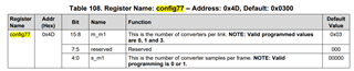
Q1) Is it correct to set the m_m1 value of Config77 to 0x3 (4 converters) to use Dual Channel (CH A / CH D only)?

Q2) Unlike CHA, CH D still has no output. Please review if there is a problem with the register settings below.

[DAC37j82] setting

               0      1       2      3      4      5      6      7      8      9      A      B      C      D      E      F

0x0000: 0018 0803 2082 A301 F0F0 FF07 F0F0 2502 0000 0000 0000 0000 0400 0400 0400 0400

0x0010: 0000 0000 0000 0000 0000 0000 0000 0000 0000 0000 0026 0000 0000 0000 9999 0000

0x0020: 8008 0000 1B39 01FF 0020 2000 0000 0000 0003 FFFF 0000 0000 0000 0001 FFFF 0004

0x0030: 0000 1000 0000 0000 0003 0000 0000 0000 0000 0000 0000 0800 0028 0088 0108 0000

0x0040: 0000 0000 0000 0000 0000 0000 0044 190A 31C3 0000 0F01 0801 1F03 0300 0F0F 1C61

0x0050: 0000 00DC 00FF 0000 00FC 00FF 0000 00FF 00FF 0000 00FF 00FF 0000 0000 0000 0123

0x0060: 4567 0211 0000 0000 0000 0000 0000 0000 440A B70B 7A07 6F02 0007 00F0 0000 0000

0x0070: 0000 0000 0000 0000 0000 0000 0000 0000 0000 0000 0000 0000 0000 0000 0000 800A

Thank you.

JH

  • JH,

    1. What are the LMFS settings used?

    2. What output channels do they plan on using? Any of the four are available but only two input data paths are allowed.

    3. If using the TI EVM, send screen shots of the GUI with their setup.

    Regards,

    Jim

  • Jim,

    Here are the customer responses.

    1.: 4211

    -. Added setting information

    DAC Data Rate input : 983.04Mhz

    Interpolation : 1

    Dac Output rate : 983.04Mhz

    FPGA Jesd CLK : 245.76Mhz

    Jesd Line Rate : 9.8304Ghz

    Path setting : config34, (1B39)

    Sample 0  -> Path a  -> DAC A

    Sample 1  -> Path b  -> DAC D

    Sample 2  -> Path c  -> DAC C (sleep)

    Sample 3  -> Path d  -> DAC B (sleep)

    2. : A & D DAC (2ea)

    Any of the four are available but only two input data paths are allowed.

    : DAC input : Rx0, Rx1, Rx2, Rx3 (Rx4~Rx7 not used), output A / D (B/C dac sleep)

    3. : Unfortunately, we use our own board. Please refer attachment(cfg file) except lmk04808 register. (it’s hard typing our dac register writing)

    cfg file is attached. Please refer to the DAC settings only.

    421_CHA_CHD_230614_register.cfg

    Thank you.

    JH

  • JH,

    Try this attached config file for the DAC. This use a K of 20 and SYSREF frequency of 6.144MHz. All other parameters match the ones mentioned above. 

    Regards,

    Jim

    DAC37J82_4211_983.04_CHA_CHD.cfg

  • Hi Jim,

    Here is the customer's answer.

    --------------------------------------------------------------------------------------------------------------------------------------------------------------------------------------------------------

    After changing to K=20, SYSREF=6.144MHz, I tested it, but the result is the same.

    If the value of Config77 (0x4D, Number of converters per link) is 0x0001, both outputs do not come out, and if it is 0x0003, A output comes out.

    Please answer whether it is correct to set 0x0003 even when using Dual CH.

    For reference, our current k setting is 32, and SYSREF is 3.84Mhz.
      SYSREF = 9.8304GHz (line rate) / (32(K)*80(N)) = 3.84MHz

    If I set 0x4D to 0x0003 with the above setting value, DAC A Output comes out.
    Additional: SYSREF Alarm OK (DAC Register Alarm 0x6C), Line Alignment OK (DAC Register Alarm 0x64, 0x65, 0x66, 0x67)

    I think that the reason why the D output is not coming out is the Path setting problem. Please comment on this.

    --------------------------------------------------------------------------------------------------------------------------------------------------------------------------------------------------------

    Regards,

    JH

  • JH,

    Config77 (0x4D) needs to be 0x100. The value entered into the register for M is M-1. For F, the value entered is F-1.

    So with LMF = 421, M= 2 and F = 1.

    M-1 = 2-1 = 1. So bits 15:8 = 00000001 

    F-1 = 1-1 = 0. So bits 4:0 = 0000

    Bits 7:5 are reserved and set to 000. 

    So address 0x4D should be 0000 0001 0000 0000 = 0x0100.

    This is the value present in the configuration file I sent.

    Regards,

    Jim 

  • Hi Jim,

    Here is the customer answer.

    ------------------------------------------------------------------------------------------

    I agree with your comment that 0x0001 should be written for 0x4D.
    Since M=2, I thought 0x0001 was correct. However, in the setting of 0x0001, there is no output.
    It was confirmed that output came out from A and D only when it was 0x0003. (Confirmed that D output is also output through changing the path setting)
    Is there any expected problem if I use 0x0003 instead of 0x0001?

    Could you please explain the difference in DAC behavior depending on settings 0x0001 and 0x0003?

    ----------------------------------------------------------------------------------------------

    Thanks,

    JH

  • JH,

    The only data value options for bits 3:0 of address 0x4D per the data sheet are 0x01 and 0x00. I do not know what 0x0003 will do as this is not a valid entry and should not be used. Also, since this device can only operate with two converters, M is always 1. So bits 15:8 of address 0x4D must be set to 0001.

    So the final value of address 0x4D must be 0x0100 for this customer's setup.

    Regards,

    Jim