This thread has been locked.

If you have a related question, please click the "Ask a related question" button in the top right corner. The newly created question will be automatically linked to this question.

ADS131M06: Analysis for 3-Phase Energy Meter

Part Number: ADS131M06

Hello.

We are needing to develop a project of an IoT, Wifi + BLE + LoRa, 3-phase energy meter. The project is a voltage, current and energy meter for industrial machines.  After several researches about what to use for the analog hardware, I found that the IC of Texas Instruments ADS131M06 is a very good choice.

For the analog hardware, I did an initial schematic, just for study and to post here in the forum, to check what the engineers of TI could say about it, and also I would like to ask some questions. My current schematic is attached in PDF. In the schematic, it is shown the circuits only for one current input and for one voltage input. After the circuit is defined, I will multiply it for 3 currents and 3 voltages.

I have put the numbers and some explanation directly on the schematic. 

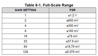
The PGA would be set for a gain of 8 in all the 6 input channels, in which the full-scale range is +- 150mV, and in which the input impedance is >= 1 M Ohms according to what is shown in the first page of the datasheet.


The following is important to highlight: we don't need so much precision on the measurements. 16 bits would be enough, 18 bits would be more than enough. This means that, even if the conversions are always 24 bits, we could discard and not consider the 8 or 6 least significant bits in the firmware. For us, one of the main advantages of this IC of TI, ADS131M06, is that it has 6 differential inputs, and that they are sampled at the same instant/moment. 

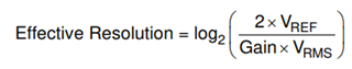
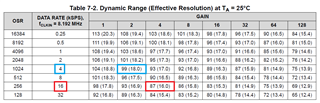
Then, regarding what is written above, about the resolution, I did not understand the table that is shown on the datasheet on page 18/109, I mean about the "Effective Resolution". I will place this table below. The preference would be for a faster sample rate, of 16k or 32k samples/s, so according to the table below I have understood that to simplify the things, if I choose a 16k sample rate, the effective resolution will be of 16 bits. I am a little unsure about this table, could you give me, please, some extra explanation?

My last question is about my schematic. The voltage reference is the internal 1.2V +- 0.1%. If I set all 6 inputs with a PGA gain of 8, the full-scale range will be +- 150mV, then, how many microvolts each bit, bit 23 (MSB) to bit 0 (LSB), of the conversion result, will represent? Or maybe, how many microvolts each unit of the value of the ADC result will represent? This will depend on the resolution, but I have doubts about it and I am unclear to express it at the moment.

I'm sorry if I could not be clear in my post, we can discuss more with the time.

Regards,

PCB-EM1-B.pdf

  • Hi ,

    The RMS noise is used for effective resolution calculation, please see the following formula in the M06 datasheet. The higher data rate, the higher noise, the worse or lower effective resolution. There is another specification, noise-free resolution, that is considered with peak-peak noise. Usually Noise Free Resolution (bits) = Effective Resolution–2.7 bit.

    The size of one code (LSB) can be calculated from the following formula:

    Your schematic looks good to me, you have differential capacitor, but you do not have a common-mode capacitors which are recommended, see the details for the anti-aliasing filter design and component selection in the following FAQ:

    [FAQ] Delta-sigma ADC anti-aliasing filter component selection

    Regards,

    Dale

  • Hello Dale.

    The line of highest frequency which will be measured is a 60Hz one.

    The period in microseconds of a complete cycle is 1/60*10^6 =  16666.6666us.

    The sampling rate that I pretend to use is 16k samples/s. The period between 2 samples, in microseconds, is to be 1/16000*10^6 = 62.5 microseconds.

    If I do the division 16666.6666 / 62.5, results ~ 266.6 samples for each individual cycle, and around 133 samples for each semi-cycle.

    The sample rate will be 16kSPS, the fCLKIN will be 8.192MHz, then according to the picture below, the OSR will be 256 and the effective resolution is 16 bits.

    On the datasheet page 21/109 is said that fMOD is the delta sigma modulator frequency, which is fCLKIN / 2, so fMOD = 8.192MHz / 2 = 4.096MHz.


    I have read the link you provided. Please check the picture below. I know what the ODR is, which will be 256, but I could not find the value of "fc-DIGITAL" on the datasheet of ADS131M06.

    At page 81/109 is shown below, that the resistors of 1K with Cdiff of 10nF are sufficient for CLKIN frequencies between 2 MHz and 8.2 MHz, and my fCLKIN will be 8.192MHz.


    Continuing to the end of the link you provided, it shows the calculation for Ccm.

    Ccm can be calculated as Ddiff divided by 10, then Ccm would be 1nF.

    Maybe this way I can finish this step of the hardware design, considering 2 series resistors of 1K, one Cdiff of 10nF, and 2 Ccm of 1nF. I say this because my knowledge of the architecture of ADCs is very limited. 

    Then, to continue, you have posted the picture below.


    +FSR = 150mV = 150.000uV = 150.000.000nV

    2^23 = 8.388.608

    150.000.000nV / 8.388.608 =  17.8813934326171875 nV / LSB

    Now talking about other things, this is what we currently plan to do on firmware.

    We will have the following (final) variables for each phase.

    Voltage RMS

    Current RMS

    Average Power

    Energy

    For each phase, there will be 16.000 measures of instantaneous voltage and current in a period of 1 second. We want to calculate these parameters above for each second, with an update every 1 second. For each individual voltage and current measurement, which is done simultaneously, by multiplying them we have the instantaneous power at the moment of the measurement. In a period of 1 second, each measurement of instantaneous voltage and current, we square each one, sum all them, and divide by 16.000, or by the actual number of readings, this way we will get the values of RMS voltage and RMS current for that period of 1 second. We can make a calculation of the average power of each 1 second period, by summing all instantaneous power measurements/calculations and dividing by 16.000 , or by the actual number of readings. And also for a period of 1 second, we can take the average power of that 1 second and add to the energy accumulator, dividing it by 3600 (3600 seconds is 1 hour), so we will have the value of power consumption in Wh. 

    Regards.

  • Hi ,

    I will look into the details and get it back to you soon.

    Regards,

    Dale

  • Hello.

    Just an update for you.

    Here is my current schematic.

    Regards.

    6787.PCB-EM1-B.pdf

  • Hi Jeferson,

    Thanks for your information. Please see my comments below:

    • Your input signal is +/-150mV, so the FSR should be 2*150mV=300mV for your LSB calculation.
    • Your actual Gain is 8, so you can refer to the Effective Resolution (ER) 15.8 bits at Gain=8 in the table 7-2, not the ER at Gain=4. As you can see the ER in the table 7-2, the higher OSR, the lower noise and the higher ER. 
    • The datasheet of ADS131M06 does not show the fc-DIGITAL" that is the bandwidth of the internal digital filter, but it can be estimated for a Sinc filter as "data rate/(Sinc filter order+1)". Since M06 has a Sinc3 filter, so it is equal to 4khz at the data rate of 16ksps you have chosen.
    • The bandwidth (fC-DIFF) of  your differential filter is around 8khz based on the 1kohm resistor and 10nF capacitor you selected, this is lower than the recommendations in the FAQ.
    • Your schematic looks good to me. You can also refer to the schematic of M08EVM board in the EVM User Guide.

    Degards,

    Dale

  • Hello Dale, thanks!

    If you think the schematic looks ok, then ok, I will keep this schematic.

    Could you calculate and tell me what will be the equivalent in uV or nV per LSB of the conversion result? Then I can calculate here to check if I get the same result. I think that's my last question.

    Regards,

  • Hi Jeferson,

    Your calculated result is correct because you used 2^23 instead of 2^24, but the FSR is full-scale range that is actually 300mV in your case.

    • FSR = 2*150mV = 300mV
    • 2^24 = 16777216
    • 1 LSB = FSR / 2^24 = 300mV / 16777216 =  17.88nV 

    Regards,

    Dale

  • Hello Dale.

    Thank you very much.