This thread has been locked.

If you have a related question, please click the "Ask a related question" button in the top right corner. The newly created question will be automatically linked to this question.

ADS112C04: No address response

Part Number: ADS112C04
Other Parts Discussed in Thread: INA228, INA233, ADS122C04,

Good Afternoon

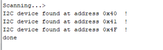
I am having difficulty with I2C addressing of this chip, i have INA233 x 2 and INA228 on same bus, all working perfectly but i also have three of the ADS112co4 chips, configured by A0 A1 as address 0x43,0x44 and 0x45

INA chips 0x40,0x41 and 0x4F

The ads chips just return a nak signal, no other response, pull ups are 1K as per datasheet to 3V3 at 100K standard speed. All pcba mounted no prototype setup

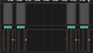
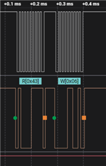
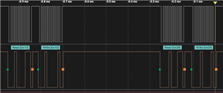
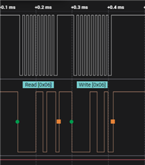
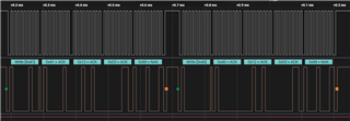
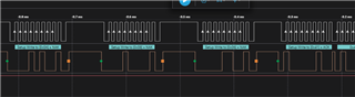
So as in the image three address's with NAK 4th address ok with ACK and accepting many more configuration bytes. So why? 

very puzzling

regards

Andy

  • Hi Andy,

    You are getting a NAK because you are not correctly communicating to the device.  The communication must be within the Start/Stop frame.  The first three communications shown are 0x0A, 0x08 and 0x06.  Here it is not clear what your intentions are.  0x08 is the START/SYNC command and 0x06 is the RESET command but there is no device being addressed.  As an example let's use the START/SYNC command which would require the following actions when communicating to device at address 0x43.

    • Issue the I2C START
    • Transmit to device 0x43 a device write (0x86)
    • Transmit the START/SYNC command (0x08)
    • Issue I2C STOP

    Follow the datasheet information in section 8.5.3 for the other commands.

    Best regards,

    Bob B

  • Tried what you suggested

      But analyzer shows 0x86 plus nak. No further data goes out

    same code different chip andaddress works fine

  • Hi Andy,

    I guess I need some further explanation as to what you are seeing and actual detail in the logic analyzer shots.  In your original description I have the following:

    The ads chips just return a nak signal, no other response
    So as in the image three address's with NAK 4th address ok with ACK

    But in the logic analyzer shots all I see is the first three bytes transmitted there is no address at all and the 4th byte is an address for the INA.  In the logic analyzer shot you can see that each of the first three bytes are bounded by a START condition (green dot) and a STOP condition ( orange dot).

    In your last post you did not give me any logic analyzer shots for me to determine what might be happening.  As to the communication, if there is a read from the ADS122C04 the micro sends the ACK/NACK.  So I really need to see the actual complete data transfer to know what is going on.

    In your first post you noted that the "ads" chips (and I assumed all of them) were responding the same way.  In this last post you mentioned you replaced a chip and now it is working fine.  I'm glad to hear you were able to finally communicate, but there must be some other issue related to the logic analyzer shot you sent in the original post.

    It would seem to me that if you made no changes to the code, but replacing a device allows it to function, then there is an issue with how you are handling a NACK condition if it stalls the communication to the other two ADC devices.  It is also possible that the ADC was not soldered correctly or that perhaps there was a solder bridge between pins.  Replacing the device allowed for the correct connections.

    In the end I'm not getting a complete story of the situation.

    Best regards,

    Bob B

  • Hi bob, sorry for delay, been very ill last two weeks, but back on the job now.

    Still getting NAK, 

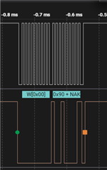
  •   So i can see a start condition (i think) then the address (hardwired ic to 0x45) but not matter what i do i get a NAK

    I have three chips with separate address's hard wired, 0x43 0x44 0x45 and all i get is NAK, but an i2c scan of my six chips on the bus reveals only three address's 0x40 0x41 and 0x4F all report back fine. your thoughts please?

    regards

    Andy

  • Serial.print("Temperature Sensor 1 U2-T1 = ");
    Wire.beginTransmission(0); // transmit to device (0x45) START CONDITION
    Wire.write(0x90); // SLAVE address
    // Wire.write(6); // RESET
    // Wire.write(8); // START
    // Wire.write(16); // RDATA
    // Wire.write(0x45); // READ MODE
    // Wire.requestFrom(69,2,true);
    // data0 = Wire.read();
    // data1 = Wire.read();
    // Wire.write(2); // POWERDOWN
    Wire.endTransmission(0); // stop transmitting
    Serial.print(data0);
    Serial.print(" ");
    Serial.print(data1);
    Serial.print(" C \n");

  • Hi Andy,

    Glad to hear you are feeling better.  I think that you may lack some understanding on how I2C works as it relates to the code you are using.  Note that in the first byte transmitted you should be showing the address for the device and whether it is a read or a write.  The second and remaining bytes would be data.

    In the last logic analyzer shots you show that you are writing 0x00 followed by 0x90.  So you are actually sending the general call address followed by 0x90 which is not a valid general call command.  So in the end you are not correctly interpreting and using the function calls correctly in your code. 

    Arduino reference

    So you need to make sure you are using the correct commands and addressing the devices correctly.  So if you want to write to the device, you would use the commands that you are showing but with the proper values.  The address goes inside of the function call for beginTransimission(). Don't use 0, but instead the device address you are actually writing to and then you should receive an ACK.

    Best regards,

    Bob B

  • Bob, If i cannot resolve this by Friday then this part will be removed from the project, time is not available now.

    the code as it stands now,

    Serial.print("Temperature Sensor 1 U2-T1 = ");
    Wire.beginTransmission(0x90); // transmit to device (0x45) START CONDITION
    Wire.write(0x90); // SLAVE address
    Wire.write(6); // RESET
    Wire.write(8); // START
    Wire.write(16); // RDATA
    Wire.write(0x90); // READ MODE
    Wire.requestFrom(144,2,true);
    data0 = Wire.read();
    data1 = Wire.read();
    Wire.write(2); // POWERDOWN
    Wire.endTransmission(0x90); // stop transmitting
    Serial.print(data0);
    Serial.print(" ");
    Serial.print(data1);
    Serial.print(" C \n");

    Serial.print("Temperature Sensor 2 U2-T2 = ");
    Wire.beginTransmission(0x88); // transmit to device (0x44)
    Wire.write(0x88); // SLAVE address
    Wire.write(6); // RESET
    Wire.write(8); // START
    Wire.write(16); // RDATA
    Wire.write(0x88); // READ MODE
    Wire.write(2); // POWERDOWN
    Wire.requestFrom(136,2,true);
    data0 = Wire.read();
    data1 = Wire.read();
    Wire.write(2); // POWERDOWN
    Wire.endTransmission(0); // stop transmitting
    Serial.print(data0);
    Serial.print(" ");
    Serial.print(data1);
    Serial.print(" C \n");

    Serial.print("Temperature Sensor 3 U2-T3 = ");
    Wire.beginTransmission(0x86); // transmit to device (0x43)
    Wire.write(0x86); // SLAVE address
    Wire.write(6); // RESET
    Wire.write(8); // START
    Wire.write(16); // RDATA
    Wire.write(0x86); // READ MODE
    Wire.requestFrom(134,2,true);
    data0 = Wire.read();
    data1 = Wire.read();
    Wire.write(2); // POWERDOWN
    Wire.endTransmission(0); // stop transmitting
    Serial.print(data0);
    Serial.print(" ");
    Serial.print(data1);
    Serial.print(" C \n");
    Serial.print(" ");
    Serial.println();

    and the screen shot response of the above code which when i perform an I2C scan still does not return an address response while the INA chips do at 40,41 and 4F, nothing from TI chips.

  • Hi Andy,

    Unfortunately what you are asking me to do is to teach you the I2C protocol and how it is to be used with Arduino.  The issues you are having are not related to the ADS112C04, but rather with how to use Arduino to communicate.  The logic analyzer shots are all you need to use to determine what you are doing incorrectly with the transfer.  All communication must have the START condition and end with a STOP condition.

    The byte transmitted following the START condition is the address to the device you are attempting to communicate with and the least significant bit indicating whether or not you are writing something to the device or are reading something from the device.  You cannot mix reads and writes in a single transaction unless a REPEATED START condition is used.  Apparently from the code and analyzer shots you are attempting to mix reads and writes within the same communication transaction.

    The logic analyzer shots do not match the code so something is missing.  Let's look at the last plots you sent.  Here we see the following in the first part of the plot:

    1. START condition
    2. Write 0x41 (ACK) - communication begins with device 0x41 and LSB is low indicating a write
    3. Write 0x41 (ACK) - Not sure what the intent is here but it becomes a register write to register 0
    4. Write 0x12 (ACK) - This is the data that gets written to register 0
    5. Write 0x03 (ACK) - This command will place the device into power-down mode
    6. Write 0x88 (NACK) - This is an invalid command and that is why you see a NACK
    7. STOP condition

    So the write values transmitted must be valid commands.  Also, it is not a good idea to send back to back commands where some time is required to complete the first command such as RESET.

    The plots earlier are meaningless.  You cannot just read or write a value.  You must first address the device you are attempting to communicate with and then issue the command.

    In my previous response I sent a link to the wire commands for Arduino.  The following is for writing to the device:

    The following function formats the transfers for writing to the address of the device to communicate with:

    Do not send a read() request here, only write() and end with endTransmission() which can also issue the STOP condition.

    To read data from the device you need to follow the communication sequence in the datasheet by using the above sequence with a command to read the conversion data which is 0x10 (actually the least significant nibble can be any value) followed by the STOP condition or a repeated START.  You can read from the device by using the function requestFrom().

    You would use the read() function in conjunction with the requestFrom() function.

    So in the end you need to understand the Arduino functions to adequately communicate properly with the ADC.  This will be true regardless of using the ADS112C04 or some other device.

    I would highly recommend just reading register data first, then progressing to writing register data and reading it back, and then using commands to START/SYNC conversions, etc.  Do not create a series of commands back to back, but instead take one step at a time until you get it working as expected.

    You do not need to issue the RESET command as the device is automatically reset on power-up.

    Best regards,

    Bob B

  • Bob, address's 0x40 0x41 and 0x4F are for the INA233 x2 and INA228 chips and are responding correctly when read, so i think there is confusion there. As a highly experienced electronic design engineer I am not asking you to teach me i2c, i am asking you to explain why your chips do not respond at all, they are on address's 0x43 0x44 and 0x45. using the arduino i2c scanner code supplied in the compiler examples on its own, no code of mine involved the scan returns three address's for the INA chips and nothing for the TI chips. pull ups are as per datasheet at 1K at 100K standard speed. Exactly the same result if i use my code.

    i have written code for sensors, rtc's and other chips many times and have never in 40 years of doing it had a chip that will not respond when polled, so i conclude that as the orientation and circuitry are correct, then i have a possibility of a bad tube of chips. 

    Having tried multiple iterations of code, the same result, INA chips respond, TI chips do not.

    Electrically all connections bell out perfectly, and even setting up one chip there is no response. 

  • Hi Andy,

    All I can say is every logic analyzer shot you have provided is wrong with respect to I2C protocol.  Not once have you shown me where you have correctly addressed the ADS112C04 devices.  So let's go back to the scanner.  It looks like you are using a Saleae logic analyzer.  Can you record, export and attach the plot file for the scanner results?  I would like to compare the plots for the working devices to the non-working devices.

    I'm obviously fixated on the code itself, and the scanner results should help clarify for me.   If the ADS112C04 devices are truly not responding at all, then it would be helpful to see a schematic.  For the device to communicate, the RESET pin must be pulled high, and both the AVDD and DVDD must be at nominal operating voltage.

    Best regards,

    Bob B