DAC43401-Q1: Want to know the right register for my situation

Part Number: DAC43401-Q1
Other Parts Discussed in Thread: DAC43401

My chip has 0x48 slave address and NVM has some settings so I reset settings right after booting.

I don't use any PMbus function.

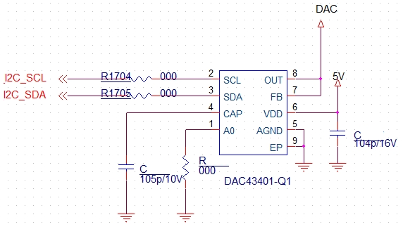
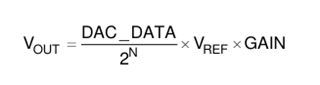
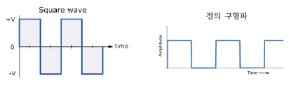
Chip VDD input is 5V and I want to make sqaure wave 0~1.8v

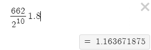
We have CAP to activate LDO to use "REF_EN" internal reference and using "DAC_SPAN" gain 1.5X  (1.21 * 1.5 = 1.8v). -> D1 register [2:0]

Below is settings that what I mentioned upper and these settings followed the sequence with #.

#1. 0xD3 -> 0x5208 : to reset settings right after booting

#2. 0x25 -> 0x0170 : DAC_MARGIN_HIGH

#3. 0x26 -> 0x0000 : DAC_MARGIN_LOW

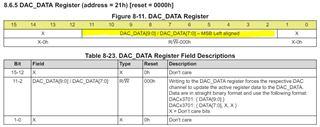
#4. 0xD1 -> 0xC1E4 : Turn on DAC with GENERAL_CONFIG

#5. 0xD3 -> 0x0108 : Start function generator

Are these settings right? Please check.

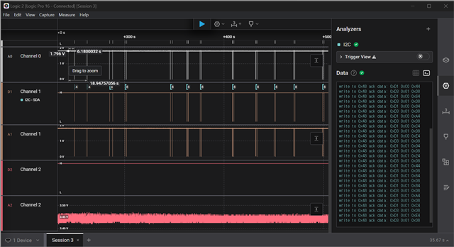
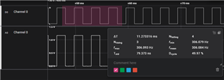
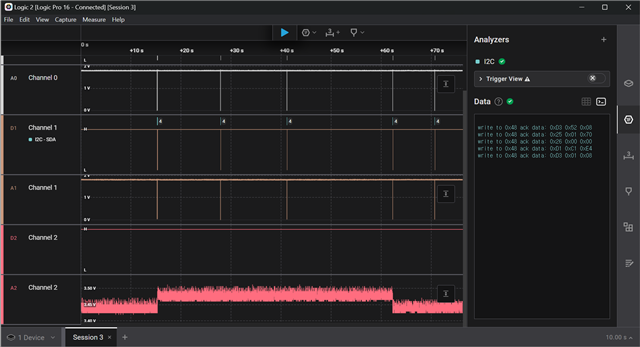
And I also attach LOGIC analyzer screenshot.

One question I have.

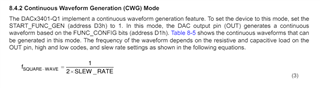
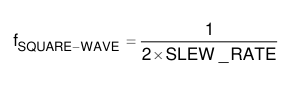
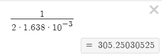
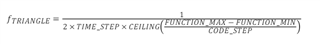
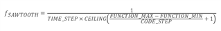
How can I set duty cycle? How can I set time for 1 cycle?

Thanks.

  • I tested to change SLEW_RATE and there's no differences.

    Thanks.

  • This is the circuit

  • Hello,

    I'm reviewing this now and will get back to you shortly.

    Best,

    Katlynne Jones

  • Hello, 

    The frequency of the square wave is determined by the SLEW_RATE field per this equation:


    You have left the SLEW_RATE field at the default, so you should update that field to get the frequency you require. The duty cycle is fixed to 50%. The rest of your settings look correct. 

    If you would like more frequency options, or a duty cycle other than 50% you will need to make a modification to your schematic, but if this is the case, the amplitude of the square wave will be fixed from 0 to DAC_SPAN instead of MARGIN_LOW to MARGIN_HIGH.

    Best,

    Katlynne Jones

  • I tested 2 days ago changing SLEW_RATE from 0000 to 1111 and there's no change.

    test environment is repeating below chunk, changing  0xD1 value 0xC004 ~ 0xC1E4

    yi2cset -f 9 0x48 0xD3 0x5208 w
    yi2cset -f 9 0x48 0x25 0x0170 w
    yi2cset -f 9 0x48 0x26 0x0000 w
    yi2cset -f 9 0x48 0xD1 0xC124 w -> 0xC004 ~ 0xC1E4
    yi2cset -f 9 0x48 0xD3 0x0108 w

    But, there's no changes

    Thanks.

  • DAC_UPDATE_BUSY appeared when I tested like below.


    1)
    yi2cset -f 9 0x48 0xD3 0x5208 w
    yi2cset -f 9 0x48 0x25 0x0170 w
    yi2cset -f 9 0x48 0x26 0x0000 w
    yi2cset -f 9 0x48 0xD3 0x0108 w

    yi2cset -f 9 0x48 0xD1 0xC1A4 w

    D0 -> 1014

    2)
    yi2cset -f 9 0x48 0xD3 0x5208 w
    yi2cset -f 9 0x48 0x25 0x0170 w
    yi2cset -f 9 0x48 0x26 0x0000 w
    yi2cset -f 9 0x48 0xD1 0xC1A4 w

    yi2cset -f 9 0x48 0xD3 0x0108 w

    D0 -> 1014

    Once DAC_UPDATE_BUSY bit set HIGH, it does not come down to LOW except for the cold booting method.

    Even with cold booting, sometimes 0xD0 value is 0x1014.

    Why my chip goes in "writing register not allowed" mode?

  • I tested 2 days ago changing SLEW_RATE from 0000 to 1111 and there's no change.

    test environment is repeating below chunk, changing  0xD1 value 0xC004 ~ 0xC1E4

    yi2cset -f 9 0x48 0xD3 0x5208 w
    yi2cset -f 9 0x48 0x25 0x0170 w
    yi2cset -f 9 0x48 0x26 0x0000 w
    yi2cset -f 9 0x48 0xD1 0xC124 w -> 0xC004 ~ 0xC1E4
    yi2cset -f 9 0x48 0xD3 0x0108 w

    But, there's no changes

    Thanks.

  • Hello, 

    We just returned form a holiday weekend in the US. Sorry for the delay. 

    When the function generator is running it is constantly writing new output codes to the DAC register. This is why the status returns that the DAC is busy.

    You need to update any settings before enabling the function generator in register 0xD3. 

    Please try adding a delay after the initial software reset in step 1 of your procedure to make sure all of the other instructions are being properly written to the device after the reset. 

    Best,

    Katlynne Jones

  • Hi Katlynne 

    Is it correct that DAC43401 requires a load connected to Vout (pin 8) for output to be generated?

  • Hi Jaesong, 

    No, it is not required to have a load on the output for the output to be generated. 

    Best,

    Katlynne Jones

  • Hi Katlynne

    We connected load to Vout and it appears square wave.

    I adjusted some slew rate to "1011: 1.6384 ms × 1.75 (per step)".

    I set 0x25 to 1.8v which leads to 0x0A58 but, wave potential range is not "0~1.8v"

    Its peak to peak range is 328mV.

    Also I want the wave frequency to be 60Hz, but there's no option to make 60Hz

    When I set slew rate to "1011", it makes 169Hz and I can not make under 169Hz frequency.

    How can I make 60Hz sqaure wave?

  • Currently, when I apply a forced load using a 5.1k resistor to the output stage, a square waveform is generated with a voltage level of 220mV. Is it correct that if nothing is connected to the DAC43401 Vout (pin 8), no waveform is produced?

  • Hi Jaesong, 

    No, that is not correct. I am using the following sequence with no load connected to the output (only the scope), and I see a square wave output with a high output of ~1.16V and low output of ~0V.

    0xD3 0x5208
    0x25 0x0A58
    0x26 0x0000
    0xD1 0xC104
    0xD3 0x0108 

    My scope is connected directly to the output pin, which is shorted to the FB pin.

    1.16V is expected with margin high data of 0x0A58. 0x0A58 corresponds to 10-bit data of 662 in decimal based on how the data is aligned in the register:

    Frequency is ~306Hz which is expected based on the datasheet equation:

    For the second question, to configure more output frequencies, you will need to disconnect the VOUT pin from the FB pin. Configure the desired frequency using triangle or sawtooth waveform mode using the below equations. The duty cycle is configured with the FB pin. Set the FB pin to VREF x gain x 0.5 for a 50% duty cycle. The drawback is that the square wave output of this mode is always 0V to VDD. 

    Best,

    Katlynne Jones