ADS1299EEGFE-PDK: Stuck at reading registers with Arduino Uno

Part Number: ADS1299EEGFE-PDK
Other Parts Discussed in Thread: ADS1299,

Tool/software:

Hello, I tried to build interface with ADS1299EEG front end through SPI..

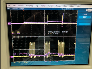
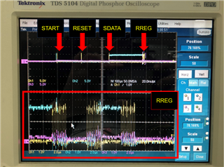
The SPI did not working.

I have gone through these 2 threads.

https://e2e.ti.com/support/data-converters-group/data-converters/f/data-converters-forum/412720/ads1298recgf-fe-stuck-at-reading-registers?ADS1298RECGF-FE-stuck-at-reading-registers

https://e2e.ti.com/support/data-converters-group/data-converters/f/data-converters-forum/1112648/ads1299eegfe-pdk-stuck-at-reading-registers

However, these still not work for me.

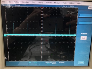
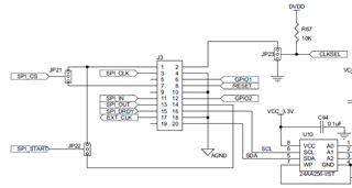
Below is my wire connection.

Arduino D13 - ADS1299 SCLK

Arduino D12 - ADS1299 DOUT

Arduino D11 - ADS1299 DIN

Arduino D10 - ADS1299 CS

Arduino D9 - ADS1299 DRDY

Arduino GND - ADS1299 J3-4(GND)

----------------------------------------------

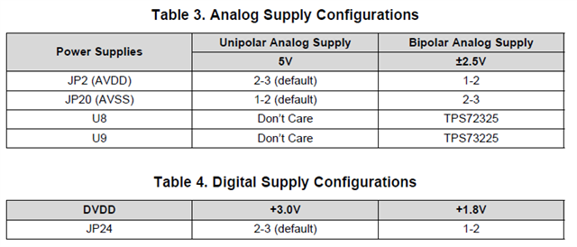
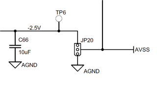
All jumpers on ADS1299 is default, and the voltage of every TP were matched the datasheet.

Did i lost something that should be connected between ADS1299 & Arduino?

  • Hello Tim,

    Thank you for your post. Can you confirm whether the nDRDY pin is toggling at the default data rate after your start-up routine is completed? What do you measure on the VCAPx pins with respect to AVSS?

    Regards,

    Ryan

  • Hello Ryan,

    Thanks for your reply.

    I would like to know how to measure the data rate of nDRDY? (It should be fCLK/8192, right?)

    I didn't see any number matched in below picture.

    Also used oscilloscope monitoring the DRDY pin on J3.

    It seems that the sampling rate of oscilloscope is too low to measure the data rate.

    Which pin should i measure on AVSS(JP21)?

    AVSS(JP21) 1-2 have jumper connected.

    I measured VCAP1(from C9) to AVSS(JP21).3,

    It's -1.31 V.

    Best regards,

    Tim

  • Hi Tim,

    The nDRDY period can be measured between consecutive falling edges. The delta-sigma modulators sample at a frequency of fCLK / 2. Assuming the default 2.048 MHz clock input, the modulator will sample at 1.024 MHz and the default output data rate will be 250 SPS (OSR = 4096). The drop-down menu in the GUI is only displaying the OSR options (fMOD / fDR = OSR). These options are also listed in the data sheet.

    AVSS should be measured on JP20 per the schematic. If JP20 is configured as [1-2], AVSS is tied to GND for unipolar supply operation. This means that JP2 (AVDD) should be configured as [2-3] = 5V. 

    When you measure VCAP1, you should measure with respect to JP20[2] (I assume JP21 is a typo). JP20[3] is the output of the -2.5-V LDO. If you instead measure VCAP1 with respect to JP20[2], you will see it is 1.19 V, which is expected.

    Regards,

    Ryan

  • Hi Ryan,

    Thanks for your explanation. As i measured DRDY pin by oscilloscope, it was 250Hz.

    Sorry for my typo, it's JP20 exactly.

    And yes, VCAP1 respect to AVSS[2] is 1.19V.

    Best regards,

    Tim

  • Hi Tim,

    It seems like the device is powering up and initializing properly. To change any registers from their default settings, you will have to first send the SDATAC (11h) command. This will exit the RDATAC mode, which automatically loads conversion data into the SPI output shift register. 

    Regards,

    Ryan

  • Hi Ryan,

    Glad to hear that my device is working properly. I will check my code again.

    Thanks for your help.

    BR,

    Tim

  • Hi Ryan,

    The datasheet says when using 500 SPS, the minimum rate of SCLK is 110k Hz(the end of p.38).

    How to calculate the minimum rate of SCLK for other SPS?


    I think i found the problem.

    In above picture, yellow is SCLK, and red is DOUT signal.

    Did the output pulses of DOUT is normal? (It's about only 1V)

    And is there anyway to adjust ADS1299 to let DOUT voltage higher?


    By the way, I found someone said that ADS1299 has digital input limit at 4.2V,.

    I searched 4.2V in datasheet by ctrl+F, but i didn't find any information.

    Is it correct that the 4.2V is the limit of ADS1299 digital input?

    BR,

    Tim

  • Hello Tim,

    The minimum SCLK frequency is calculated by Equation 9 on page 39. Basically, you need to send 216 clock pulses within one data rate period with some margin for timing delays.

    It appears that another device is loading the DOUT pin. Is nCS low during this transaction?

    Digital inputs are limited by DGND and DVDD supplies. See the Electrical Characteristics section for digital input voltage limits.

    Regards,

    Ryan

  • Hello Ryan,

    Thanks for telling me where the Equation is.

    Yes, i use Arduino Uno to catch DOUT data, and have checked that nCS is low during transaction.

    Does the input limit restrict SPI communication for ADS1299?

    Now, i'm trying reduce voltage sending to SCLK or DIN.

    Best regards,

    Tim

  • Hi Tim,

    The digital I/O high and low levels are relative to DVDD. The min and max I/O levels are shown in the data sheet. It is ok to allow SCLK to toggle from 0V to DVDD (there's no need to reduce the levels). However, I suggest to probe the SCLK signal with a scope to confirm there is no excessive over/undershoot or ringing on the clock signal.

    Regards,

    Ryan

  • Hello Ryan,

    Thanks for your advice. I thought i send SPI signal successfully. 

    I sent 4 SPI commands, and SCLK and DOUT shown correct byte pattern. However, when i sent RREG command, i did not get response from ADS1299.

    I have checked that MOSI should connect to DIN, MISO connect to DOUT, and nCS worked properly.

    (YELLOW is SCLK, BLUE is DIN signal, RED is DOUT signal)

    Is there any pin configuration on ADS1299 i do not mention?

    Best regards,

    Tim

  • Hi Tim,

    What are your master clock (CLK) and serial clock (SCLK) frequencies? Have you checked the tSDECODE timing restriction for multi-byte commands?

    [FAQ] ADS129x: What is the minimum frequency for my SCLK? - Data converters forum - Data converters - TI E2E support forums

    Regards,

    Ryan

  • Hi Ryan,

    CLK was 2.048M Hz as ADS1299 default, and SCLK was set to 4M Hz. Yes, the tSDECODE should be 4 * tCLK(, and i set 3 microseconds as delay time. So i think it's ok?

    Could you help recheck jumper setting on ADS1299EEGFE-PDK please?

    Is the first pin count from left or count from the side with JPx printed?

    Another question is i found that the voltage of DOUT changed not as my expect. I thought that if ADS1299 didn't receive commands, DOUT should be at 0 level. However, when i sending commands the voltage of DOUT change when command sent to ADS1299.

    When START command sent(BLUE), the voltage of DOUT signal(RED) had a peak value(1.7V). The baseline of DOUT was also turn up to 0.4V after START command.

    (SCLK: YELLOW;  DIN: RED;  DOUT: BLUE;  CS: GREEN)

    Below is the three bytes of RREG command.

    First, sending RREG command with register address(0010 0000)

    Second, sending 000n nnnn to read number of registers. It's 0000 0000 because i only want to read ID register.

    Third, sending a dummy bytes to receive ID register.

    Is there anything wrong during the RREG commands? In last 2 pictures, the signal of DOUT also turn up to 1.2V every bit sending. Why did it happen?

    At last, if above all are correct, I still can't receive any register from ADS1299 by SPI.

    Please give me more suggestion.

    Best regards,

    Tim

  • Hi Tim,

    Could you try uploading the image of your jumper settings again? The link is broken.

    Pin 1 of the JPx jumpers is usually designated by a dot in the silkscreen. Also, you can look on the bottom side and pin 1 will have a square pad, while the other pins have a circular pad.

    The change in DOUT that you see while sending SPI commands is likely noise coupling from other digital signals, most likely SCLK. Some of this error may actually be introduced by the oscilloscope probes themselves. You can try shortening the ground leads or using a logic analyzer for a cleaner signal.

    Regards,

    Ryan

  • Hi Ryan,

    Sure, if the picture is not clear, please tell me.

    Thanks for your explanation.
    According to your explanation, i think my JP2 and JP20 is not default configuration, right?

    Let me describe my setting again.
    Before using SPI interface, i had tried the software that TI build for ADS1299EEGFE. I could see correct register in the software.
    When trying SPI, i connected power supply to MMB0, and measured the test points at p.15. All TPs are matched the datasheet.
    According to datasheet, i connected SCLK, DIN, DOUT, nCS, GND to Arduino Uno for SPI communication.
    Is there any pin i missed to use SPI?

    I also have some curious points.
    Would it be MMB0 influence the SPI transmission?
    If i want to separate ADS1299 and MMB0, how do i supply power to ADS1299 and do i have to change the jumper configuration?
    How to know if ADS1299 receive my commands successfully?

    BR,

    Tim

  • Hi Tim,

    The picture did not upload.

    When interfacing the EVM directly with Arduino, I suggest that you completely remove the MMB0. Supply power directly to JP2, JP20, and JP24 (pin 2 for all) without the jumpers. Also share the Arduino board GND to a GND test point on the ADS1299 board. For the SPI signals, you may find that some are available directly on J3, while others pass through a jumper (i.e. nCS connects to JP21). Make sure you are connecting the signals at a point which directly connects to the ADS1299 pins.

    I would also add a connection for nDRDY to an interrupt pin or GPIO on your controller such that you can monitor for when new conversions become available to read.

    Regards,

    Ryan

  • Hi Ryan,

    Thank you for providing the power supply method.

    I think we don't need to look at the pictures in previous reply anymore. Let's focus on the way we going now.
    Today, i tried supply power directly on JP2, JP20, JP24, but i couldn't measure any voltage from test points matched datasheet.
    Below is my setting.
    Orange and red jumper wire connect to JP2, and JP20. Yellow is 3V supply to JP24. GND connects to TP12(To my understanding, all black TPx on the board is the same GND).
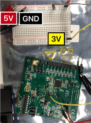
     (It's not real work, please ignore the 3V without power supply. I will use a voltage regulator or divider to lower the 5V input and supply to JP24).

    Is there anything i did wrong? 

    "For the SPI signals, you may find that some are available directly on J3, while others pass through a jumper (i.e. nCS connects to JP21). Make sure you are connecting the signals at a point which directly connects to the ADS1299 pins."

    According to above, it means i can not use the pins on J3 if the pins directly connects to ADS1299, right?

    BR,

    Tim

  • Hello Tim,

    If you are connecting +5V to AVDD (JP2.2), Then you must connect AVSS to AGND (JP20[1-2]). This is explained in the EVM User Guide section 4.1.

    You can use any pin on J3 to connect external interface signals. However, if the signal passes through a jumper, then you must ensure the jumper is configured correctly. For example, connect nCS to J3.1 and configure JP21 in the [1-2] position. 

    Regards,

    Ryan

  • Hi Ryan,

    Appreciate for your help and patience. I have made it work!

    I successfully received register by SPI with Arduino.

    Have a nice weekend!


    I would like to leave some message for those who encountered same issue.

    (I will use ADS1299FE instead of ADS1299EEGFE in below description.)

    First, I used ADS1299EEGFE connected with MMB0.
    Power MMB0 by wall adapter jack.(ADS1299FE user guide 9.4)

    Check all test points in section 4.1 table2.

    Check jumper configuration on ADS1299FE.
    You can find default setting in section 2.5 table1.
    The first pin for every jumper is from the side of below symbol.
              __________
             |                    \
    last   |        pin        | first
             |__________ /

    If you want to use J3[7] for nCS, you have to change JP21[1-2] to JP21[2-3].
    I missed this information untill i found this thread(https://e2e.ti.com/support/data-converters-group/data-converters/f/data-converters-forum/318293/no-signal-from-the-dout-pin-in-ads1299-eeg-fe).


    Best regards,

    Tim

  • Hi Tim, 

    I'm glad to hear everything is working now. Thanks for the feedback!

    Regards,

    Ryan