Other Parts Discussed in Thread: MSP432E401Y, , ADS131M08
Tool/software:
Hi,
I have the ADS131M08EVM, in which I have removed R67. The AVDD and DVDD are connected to a 3V3 output from a MSP432E401Y Launchpad. The connections to the launchpad from the Pinout of the ADS EVM are provided as given in the sample code in SBAC254.zip (ADS131M0x Example Code). Please see the commented pin connections (from lines 16) in the code below. DIN from the ADS EVM is given to PQ2 (MOSI) and DOUT to PQ3 (MISO).
/*

1. Make all the hardware connections in the ADS board. SYNC/RESET, CS, DRDY, DIN, DOUT, AVDD, DVDD, GND.

2. This is a check code. There is a function called adcStartup(), in which one register is read back.

3. Ensure that the valuse read back is correct as per the datasheet and then proceed to have your code
  written after this function.

The functions are referred from an existing code example from TI.
*/


//****************************************************************************
//
// LaunchPad pinout...
//
//****************************************************************************
//
//                  LEFT                                RIGHT
//               /--------\                          /--------\
//        +3.3V -|3V3  +5V|- +5V                CLK -|PG1  GND|- GND
//              -|PD2  GND|- GND       nSYNC/nRESET -|PK4  PM7|-
//              -|PP0  PB4|-                    nCS -|PK5 *PP5|-
//              -|PP1  PB5|-                  nDRDY -|PM0  PA7|-
//              -|PD4  PK0|-                        -|PM1  RST|-
//              -|PD5  PK1|-                        -|PM2  PQ2|- DIN
//         SCLK -|PQ0  PK2|-                        -|PH0  PQ3|- DOUT
//              -|PP4* PK3|-                        -|PH1 *PP3|-
//              -|PN5  PA4|-                        -|PK6  PQ1|-
//              -|PN4  PA5|-                        -|PK7  PM6|-
//               \--------/                          \--------/
//


#include <stdint.h>
#include <stdbool.h>
#include "ti/devices/msp432e4/driverlib/driverlib.h"
#include "ads131m0x.h"

uint32_t systemClock;
uint32_t register_value;

// Flag to indicate if a /DRDY interrupt has occurred
static volatile bool flag_nDRDY_INTERRUPT = false;

#define SSI_BASE_ADDR       (SSI3_BASE)

//*****************************************************************************
//
// The error routine that is called if the driver library encounters an error.
//
//*****************************************************************************
#ifdef DEBUG
void
__error__(char *pcFilename, uint32_t ui32Line)
{
    while(1);
}
#endif

//*****************************************************************************
//
// Main Function. All other functions are written down
//
//*****************************************************************************
int main(void)
{
    // IMPORTANT: Make sure device is powered before setting GPIOs pins to HIGH state.

    // Initialize GPIOs pins used by ADS131M0x
    InitGPIO();

    // Initialize SPI peripheral used by ADS131M0x
    InitSPI();
    while(1)
    {
        // Run ADC startup function
            adcStartup();

    }
//    // Run ADC startup function
//    adcStartup();


}

//*****************************************************************************
//
//! Configures the MCU's GPIO pins that interface with the ADC.
//!
//! \fn void InitGPIO(void)
//!
//! \return None.
//
//*****************************************************************************
void InitGPIO(void)
{

    /* Enable the clock to the GPIO Port K and wait for it to be ready */
    MAP_SysCtlPeripheralEnable(SYSCTL_PERIPH_GPIOK);
    while(!(SysCtlPeripheralReady(SYSCTL_PERIPH_GPIOK)))
    {
    }

    /* Configure the GPIO for 'nSYNC_nRESET' as output and set high */
    MAP_GPIOPinTypeGPIOOutput(nSYNC_nRESET_PORT, nSYNC_nRESET_PIN);
    MAP_GPIOPinWrite(nSYNC_nRESET_PORT, nSYNC_nRESET_PIN, nSYNC_nRESET_PIN);

    /* Configure the GPIO for 'nCS' as output and set high */
    MAP_GPIOPinTypeGPIOOutput(nCS_PORT, nCS_PIN);
    MAP_GPIOPinWrite(nCS_PORT, nCS_PIN, nCS_PIN);

    /* Enable the clock to the GPIO Port M and wait for it to be ready */
    MAP_SysCtlPeripheralEnable(SYSCTL_PERIPH_GPIOM);
    while(!(SysCtlPeripheralReady(SYSCTL_PERIPH_GPIOM)))
    {
    }

    /* Configure the GPIO for 'nDRDY' as input with falling edge interrupt */
    GPIOIntRegister(nDRDY_PORT, GPIO_DRDY_IRQHandler);
    MAP_GPIOPinTypeGPIOInput(nDRDY_PORT, nDRDY_PIN);
    MAP_GPIOIntTypeSet(nDRDY_PORT, nDRDY_PIN, GPIO_FALLING_EDGE);
    MAP_GPIOIntEnable(nDRDY_PORT, nDRDY_PIN);
    MAP_IntEnable(nDRDY_INT);
}

//*****************************************************************************
//
// Interrupt handler for nDRDY GPIO
//
//*****************************************************************************


//*****************************************************************************
//
//! Interrupt handler for /DRDY falling edge interrupt.
//!
//! \fn void GPIO_DRDY_IRQHandler(void)
//!
//! \return None.
//
//*****************************************************************************
void GPIO_DRDY_IRQHandler(void)
{

    // Possible ways to handle this interrupt:
    // If you decide to read data here, you may want to disable other interrupts to avoid partial data reads.

    // In this example we set a flag and exit the interrupt routine. In the main program loop, your application can examine
    // all state flags and decide which state (operation) to perform next.

    /* Get the interrupt status from the GPIO and clear the status */
    uint32_t getIntStatus = MAP_GPIOIntStatus(nDRDY_PORT, true);

    /* Check if the nDRDY pin triggered the interrupt */
    if(getIntStatus & nDRDY_PIN)
    {
        /* Interrupt action: Set a flag */
        flag_nDRDY_INTERRUPT = true;
    }

    /* Clear interrupt */
    MAP_GPIOIntClear(nDRDY_PORT, getIntStatus);

    // NOTE: We add a short delay at the end to prevent re-entrance. Refer to E2E issue:
    // https://e2e.ti.com/support/microcontrollers/tiva_arm/f/908/p/332605/1786938#1786938
    SysCtlDelay(3);
}

//*****************************************************************************
//
//! Configures the MCU's SPI peripheral, for interfacing with the ADC.
//!
//! \fn void InitSPI(void)
//!
//! \return None.
//
//*****************************************************************************
void InitSPI(void)
{
    //
    // Enable the clock to SSI-3 module and configure the SSI Master
    //
    MAP_SysCtlPeripheralEnable(SYSCTL_PERIPH_SSI3);
    while(!(MAP_SysCtlPeripheralReady(SYSCTL_PERIPH_SSI3)))
    {
    }

    //
    // Enable clocks to GPIO Port Q and configure pins as SSI
    //
    MAP_SysCtlPeripheralEnable(SYSCTL_PERIPH_GPIOQ);
    while(!(MAP_SysCtlPeripheralReady(SYSCTL_PERIPH_GPIOQ)))
    {
    }

    MAP_GPIOPinConfigure(GPIO_PQ0_SSI3CLK);
    //MAP_GPIOPinConfigure(GPIO_PA3_SSI0FSS); // Using GPIO for nCS instead of the FSS pin.
    MAP_GPIOPinConfigure(GPIO_PQ2_SSI3XDAT0);
    MAP_GPIOPinConfigure(GPIO_PQ3_SSI3XDAT1);
    MAP_GPIOPinTypeSSI(GPIO_PORTQ_BASE, (GPIO_PIN_0 | GPIO_PIN_2 | GPIO_PIN_3));

    /* Configure the system clock for 120 MHz */
    systemClock = MAP_SysCtlClockFreqSet((SYSCTL_XTAL_25MHZ | SYSCTL_OSC_MAIN |
                                              SYSCTL_USE_PLL | SYSCTL_CFG_VCO_480),
                                              120000000);

    // Configure: SPI MODE 1, 5 MHz SCLK, 8-bits per frame
    MAP_SSIConfigSetExpClk(SSI_BASE_ADDR, systemClock, SSI_FRF_MOTO_MODE_1,   \
                           SSI_MODE_MASTER, (systemClock/24), 8);
    //MAP_SSIEnable(SSI_BASE_ADDR);

    //
    // Enable the SSI2 module.
    //
    SSIEnable(SSI_BASE_ADDR);
    SSIAdvModeSet(SSI_BASE_ADDR, SSI_ADV_MODE_READ_WRITE);
    SSIAdvFrameHoldDisable(SSI_BASE_ADDR);

    //
    // Read any residual data from the SSI port.  This makes sure the receive
    // FIFOs are empty, so we don't read any unwanted junk.  This is done here
    // because the SPI SSI mode is full-duplex, which allows you to send and
    // receive at the same time.  The SSIDataGetNonBlocking function returns
    // "true" when data was returned, and "false" when no data was returned.
    // The "non-blocking" function checks if there is any data in the receive
    // FIFO and does not "hang" if there isn't.
    //
    uint32_t junk;
    while(MAP_SSIDataGetNonBlocking(SSI_BASE_ADDR, &junk));
}

//*****************************************************************************
//
//! Start up sequence for the ADS131M0x.
//!
//! \fn void adcStartup(void)
//!
//! Before calling this function, the device must be powered,
//! the SPI/GPIO pins of the MCU must have already been configured,
//! and (if applicable) the external clock source should be provided to CLKIN.
//!
//! \return None.
//
//*****************************************************************************
void adcStartup(void)
{
    /* (OPTIONAL) Provide additional delay time for power supply settling */
	delay_ms(50);
	setCS(LOW);
	delay_ms(2);
	/* (REQUIRED) Set nRESET pin high for ADC operation */
	setSYNC_RESET(HIGH);

	/* (OPTIONAL) Toggle nRESET pin to ensure default register settings. */
	/* NOTE: This also ensures that the device registers are unlocked.	 */
	toggleRESET();

    /* (REQUIRED) Initialize internal 'registerMap' array with device default settings */
	restoreRegisterDefaults();

    /* (OPTIONAL) Validate first response word when beginning SPI communication: (0xFF20 | CHANCNT) */
	uint16_t response = sendCommand(OPCODE_NULL);

	/* (OPTIONAL) Define your initial register settings here */
    //writeSingleRegister(CLOCK_ADDRESS, (CLOCK_DEFAULT & ~CLOCK_OSR_MASK) | CLOCK_OSR_256);

    /* (REQUIRED) Configure MODE register settings
     * NOTE: This function call is required here for this particular code implementation to work.
     * This function will enforce the MODE register settings as selected in the 'ads131m0x.h' header file.
     */
   // writeSingleRegister(MODE_ADDRESS, MODE_DEFAULT);

    /* (OPTIONAL) Read back all registers */

	/* (OPTIONAL) Check STATUS register for faults */
}


//*****************************************************************************
//
//! Provides a timing delay with 'ms' resolution.
//!
//! \fn void delay_ms(const uint32_t delay_time_ms)
//!
//! \param delay_time_ms is the number of milliseconds to delay.
//!
//! \return None.
//
//*****************************************************************************
void delay_ms(const uint32_t delay_time_ms)
{
    const uint32_t cycles_per_loop = 3;
    MAP_SysCtlDelay( delay_time_ms * systemClock / (cycles_per_loop * 1000u) );
}


//*****************************************************************************
//
//! Controls the state of the nSYNC/nRESET GPIO pin.
//!
//! \fn void setSYNC_RESET(const bool state)
//!
//! \param state boolean indicating which state to set the nSYNC/nRESET pin (0=low, 1=high)
//!
//! NOTE: The 'HIGH' and 'LOW' macros defined in hal.h can be passed to this
//! function for the 'state' parameter value.
//!
//! \return None.
//
//*****************************************************************************
void setSYNC_RESET(const bool state)
{
    uint8_t value = (uint8_t) (state ? nSYNC_nRESET_PIN : 0);
    MAP_GPIOPinWrite(nSYNC_nRESET_PORT, nSYNC_nRESET_PIN, value);
}


//*****************************************************************************
//
//! Controls the state of the /CS GPIO pin.
//!
//! \fn void setCS(const bool state)
//!
//! \param state boolean indicating which state to set the /CS pin (0=low, 1=high)
//!
//! NOTE: The 'HIGH' and 'LOW' macros defined in hal.h can be passed to this
//! function for the 'state' parameter value.
//!
//! \return None.
//
//*****************************************************************************
void setCS(const bool state)
{
    // td(CSSC) delay
    if(state) { SysCtlDelay(2); }

    uint8_t value = (uint8_t) (state ? nCS_PIN : 0);
    MAP_GPIOPinWrite(nCS_PORT, nCS_PIN, value);

    // td(SCCS) delay
    if(!state) { SysCtlDelay(2); }
}

//*****************************************************************************
//
//! Toggles the "nSYNC/nRESET" pin to trigger a reset
//! (LOW, delay 2 ms, then HIGH).
//!
//! \fn void toggleRESET(void)
//!
//! \return None.
//
//*****************************************************************************
void toggleRESET(void)
{
    setCS(LOW);
    delay_ms(5);
    MAP_GPIOPinWrite(nSYNC_nRESET_PORT, nSYNC_nRESET_PIN, 0);

    // Minimum /RESET pulse width (tSRLRST) equals 2,048 CLKIN periods (1 ms @ 2.048 MHz)
    delay_ms(20);
    MAP_GPIOPinWrite(nSYNC_nRESET_PORT, nSYNC_nRESET_PIN, nSYNC_nRESET_PIN);

    // tREGACQ delay before communicating with the device again
    delay_ms(10);
    //setCS(LOW);
    //delay_ms(5);
    // NOTE: The ADS131M0x's next response word should be (0xFF20 | CHANCNT).
    // A different response may be an indication that the device did not reset.

    // Update register array
    //restoreRegisterDefaults();

    // Write to MODE register to enforce mode settings
    //writeSingleRegister(MODE_ADDRESS, MODE_DEFAULT);
}


//*****************************************************************************
//
//! Updates the registerMap[] array to its default values.
//!
//! \fn void restoreRegisterDefaults(void)
//!
//! NOTES:
//! - If the MCU keeps a copy of the ADS131M0x register settings in memory,
//! then it is important to ensure that these values remain in sync with the
//! actual hardware settings. In order to help facilitate this, this function
//! should be called after powering up or resetting the device (either by
//! hardware pin control or SPI software command).
//!
//! - Reading back all of the registers after resetting the device can
//! accomplish the same result; however, this might be problematic if the
//! device was previously in CRC mode or the WLENGTH was modified, since
//! resetting the device exits these modes. If the MCU is not aware of this
//! mode change, then read register commands will return invalid data due to
//! the expectation of data appearing in a different byte position.
//!
//! \return None.
//
//*****************************************************************************
void restoreRegisterDefaults(void)
{
    registerMap[ID_ADDRESS]             =   0x00;               /* NOTE: This a read-only register */
    registerMap[STATUS_ADDRESS]         =   STATUS_DEFAULT;
    registerMap[MODE_ADDRESS]           =   MODE_DEFAULT;
    registerMap[CLOCK_ADDRESS]          =   CLOCK_DEFAULT;
    registerMap[GAIN1_ADDRESS]          =   GAIN1_DEFAULT;
    registerMap[GAIN2_ADDRESS]          =   GAIN2_DEFAULT;
    registerMap[CFG_ADDRESS]            =   CFG_DEFAULT;
    registerMap[THRSHLD_MSB_ADDRESS]    =   THRSHLD_MSB_DEFAULT;
    registerMap[THRSHLD_LSB_ADDRESS]    =   THRSHLD_LSB_DEFAULT;
    registerMap[CH0_CFG_ADDRESS]        =   CH0_CFG_DEFAULT;
    registerMap[CH0_OCAL_MSB_ADDRESS]   =   CH0_OCAL_MSB_DEFAULT;
    registerMap[CH0_OCAL_LSB_ADDRESS]   =   CH0_OCAL_LSB_DEFAULT;
    registerMap[CH0_GCAL_MSB_ADDRESS]   =   CH0_GCAL_MSB_DEFAULT;
    registerMap[CH0_GCAL_LSB_ADDRESS]   =   CH0_GCAL_LSB_DEFAULT;
#if (CHANNEL_COUNT > 1)
    registerMap[CH1_CFG_ADDRESS]        =   CH1_CFG_DEFAULT;
    registerMap[CH1_OCAL_MSB_ADDRESS]   =   CH1_OCAL_MSB_DEFAULT;
    registerMap[CH1_OCAL_LSB_ADDRESS]   =   CH1_OCAL_LSB_DEFAULT;
    registerMap[CH1_GCAL_MSB_ADDRESS]   =   CH1_GCAL_MSB_DEFAULT;
    registerMap[CH1_GCAL_LSB_ADDRESS]   =   CH1_GCAL_LSB_DEFAULT;
#endif
#if (CHANNEL_COUNT > 2)
    registerMap[CH2_CFG_ADDRESS]        =   CH2_CFG_DEFAULT;
    registerMap[CH2_OCAL_MSB_ADDRESS]   =   CH2_OCAL_MSB_DEFAULT;
    registerMap[CH2_OCAL_LSB_ADDRESS]   =   CH2_OCAL_LSB_DEFAULT;
    registerMap[CH2_GCAL_MSB_ADDRESS]   =   CH2_GCAL_MSB_DEFAULT;
    registerMap[CH2_GCAL_LSB_ADDRESS]   =   CH2_GCAL_LSB_DEFAULT;
#endif
#if (CHANNEL_COUNT > 3)
    registerMap[CH3_CFG_ADDRESS]        =   CH3_CFG_DEFAULT;
    registerMap[CH3_OCAL_MSB_ADDRESS]   =   CH3_OCAL_MSB_DEFAULT;
    registerMap[CH3_OCAL_LSB_ADDRESS]   =   CH3_OCAL_LSB_DEFAULT;
    registerMap[CH3_GCAL_MSB_ADDRESS]   =   CH3_GCAL_MSB_DEFAULT;
    registerMap[CH3_GCAL_LSB_ADDRESS]   =   CH3_GCAL_LSB_DEFAULT;
#endif
#if (CHANNEL_COUNT > 4)
    registerMap[CH4_CFG_ADDRESS]        =   CH4_CFG_DEFAULT;
    registerMap[CH4_OCAL_MSB_ADDRESS]   =   CH4_OCAL_MSB_DEFAULT;
    registerMap[CH4_OCAL_LSB_ADDRESS]   =   CH4_OCAL_LSB_DEFAULT;
    registerMap[CH4_GCAL_MSB_ADDRESS]   =   CH4_GCAL_MSB_DEFAULT;
    registerMap[CH4_GCAL_LSB_ADDRESS]   =   CH4_GCAL_LSB_DEFAULT;
#endif
#if (CHANNEL_COUNT > 5)
    registerMap[CH5_CFG_ADDRESS]        =   CH5_CFG_DEFAULT;
    registerMap[CH5_OCAL_MSB_ADDRESS]   =   CH5_OCAL_MSB_DEFAULT;
    registerMap[CH5_OCAL_LSB_ADDRESS]   =   CH5_OCAL_LSB_DEFAULT;
    registerMap[CH5_GCAL_MSB_ADDRESS]   =   CH5_GCAL_MSB_DEFAULT;
    registerMap[CH5_GCAL_LSB_ADDRESS]   =   CH5_GCAL_LSB_DEFAULT;
#endif
#if (CHANNEL_COUNT > 6)
    registerMap[CH6_CFG_ADDRESS]        =   CH6_CFG_DEFAULT;
    registerMap[CH6_OCAL_MSB_ADDRESS]   =   CH6_OCAL_MSB_DEFAULT;
    registerMap[CH6_OCAL_LSB_ADDRESS]   =   CH6_OCAL_LSB_DEFAULT;
    registerMap[CH6_GCAL_MSB_ADDRESS]   =   CH6_GCAL_MSB_DEFAULT;
    registerMap[CH6_GCAL_LSB_ADDRESS]   =   CH6_GCAL_LSB_DEFAULT;
#endif
#if (CHANNEL_COUNT > 7)
    registerMap[CH7_CFG_ADDRESS]        =   CH7_CFG_DEFAULT;
    registerMap[CH7_OCAL_MSB_ADDRESS]   =   CH7_OCAL_MSB_DEFAULT;
    registerMap[CH7_OCAL_LSB_ADDRESS]   =   CH7_OCAL_LSB_DEFAULT;
    registerMap[CH7_GCAL_MSB_ADDRESS]   =   CH7_GCAL_MSB_DEFAULT;
    registerMap[CH7_GCAL_LSB_ADDRESS]   =   CH7_GCAL_LSB_DEFAULT;
#endif
    registerMap[REGMAP_CRC_ADDRESS]     =   REGMAP_CRC_DEFAULT;
}


//*****************************************************************************
//
//! Writes data to a single register.
//!
//! \fn void writeSingleRegister(uint8_t address, uint16_t data)
//!
//! \param address is the address of the register to write to.
//! \param data is the value to write.
//!
//! This command will be ignored if device registers are locked.
//!
//! \return None.
//
//*****************************************************************************
void writeSingleRegister(uint8_t address, uint16_t data)
{
    /* Check that the register address is in range */
    assert(address < NUM_REGISTERS);

    // (OPTIONAL) Enforce certain register field values when
    // writing to the MODE register to fix the operation mode
    if (MODE_ADDRESS == address)
    {
        data = enforce_selected_device_modes(data);
    }

    // Build TX and RX byte array
#ifdef ENABLE_CRC_IN
    uint8_t dataTx[12] = { 0 };     // 3 words, up to 4 bytes each = 12 bytes maximum
    uint8_t dataRx[12] = { 0 };
#else
    uint8_t dataTx[8] = { 0 };      // 2 words, up to 4 bytes long = 8 bytes maximum
    uint8_t dataRx[8] = { 0 };
#endif
    uint16_t opcodes[2];
    opcodes[0] = OPCODE_WREG | (((uint16_t) address) << 7);
    opcodes[1] = data;
    uint8_t numberOfBytes = buildSPIarray(&opcodes[0], 2, dataTx);

    // Send command
    spiSendReceiveArrays(dataTx, dataRx, numberOfBytes);

    // Update internal array
    registerMap[address] = data;

    // (RECOMMENDED) Read back register to confirm register write was successful
    register_value = readSingleRegister(address);
    // NOTE: Enabling the CRC words in the SPI command will NOT prevent an invalid W
}


//*****************************************************************************
//
//! Modifies MODE register data to maintain device operation according to
//! preselected mode(s) (RX_CRC_EN, WLENGTH, etc.).
//!
//! \fn uint16_t enforce_selected_device_mode(uint16_t data)
//!
//! \param data uint16_t register data.
//!
//! \return uint16_t modified register data.
//
//*****************************************************************************
uint16_t enforce_selected_device_modes(uint16_t data)
{


    ///////////////////////////////////////////////////////////////////////////
    // Enforce RX_CRC_EN setting

#ifdef ENABLE_CRC_IN
    // When writing to the MODE register, ensure RX_CRC_EN bit is ALWAYS set
    data |= MODE_RX_CRC_EN_ENABLED;
#else
    // When writing to the MODE register, ensure RX_CRC_EN bit is NEVER set
    data &= ~MODE_RX_CRC_EN_ENABLED;
#endif // ENABLE_CRC_IN


    ///////////////////////////////////////////////////////////////////////////
    // Enforce WLENGH setting

#ifdef WORD_LENGTH_24BIT
    // When writing to the MODE register, ensure WLENGTH bits are ALWAYS set to 01b
    data = (data & ~MODE_WLENGTH_MASK) | MODE_WLENGTH_24BIT;
#elif defined WORD_LENGTH_32BIT_SIGN_EXTEND
    // When writing to the MODE register, ensure WLENGH bits are ALWAYS set to 11b
    data = (data & ~MODE_WLENGTH_MASK) | MODE_WLENGTH_32BIT_MSB_SIGN_EXT;
#elif defined WORD_LENGTH_32BIT_ZERO_PADDED
    // When writing to the MODE register, ensure WLENGH bits are ALWAYS set to 10b
    data = (data & ~MODE_WLENGTH_MASK) | MODE_WLENGTH_32BIT_LSB_ZEROES;
#elif defined WORD_LENGTH_16BIT_TRUNCATED
    // When writing to the MODE register, ensure WLENGH bits are ALWAYS set to 00b
    data = (data & ~MODE_WLENGTH_MASK) | MODE_WLENGTH_16BIT;
#endif


    ///////////////////////////////////////////////////////////////////////////
    // Enforce DRDY_FMT setting

#ifdef DRDY_FMT_PULSE
    // When writing to the MODE register, ensure DRDY_FMT bit is ALWAYS set
    data = (data & ~MODE_DRDY_FMT_MASK) | MODE_DRDY_FMT_NEG_PULSE_FIXED_WIDTH;
#else
    // When writing to the MODE register, ensure DRDY_FMT bit is NEVER set
    data = (data & ~MODE_DRDY_FMT_MASK) | MODE_DRDY_FMT_LOGIC_LOW;
#endif


    ///////////////////////////////////////////////////////////////////////////
    // Enforce CRC_TYPE setting

#ifdef CRC_CCITT
    // When writing to the MODE register, ensure CRC_TYPE bit is NEVER set
    data = (data & ~STATUS_CRC_TYPE_MASK) | STATUS_CRC_TYPE_16BIT_CCITT;
#elif defined CRC_ANSI
    // When writing to the MODE register, ensure CRC_TYPE bit is ALWAYS set
    data = (data & ~STATUS_CRC_TYPE_MASK) | STATUS_CRC_TYPE_16BIT_ANSI;
#endif

    // Return modified register data
    return data;
}


//*****************************************************************************
//
//! Builds SPI TX data arrays according to number of opcodes provided and
//! currently programmed device word length.
//!
//! \fn uint8_t buildSPIarray(const uint16_t opcodeArray[], uint8_t numberOpcodes, uint8_t byteArray[])
//!
//! \param opcodeArray[] pointer to an array of 16-bit opcodes to use in the SPI command.
//! \param numberOpcodes the number of opcodes provided in opcodeArray[].
//! \param byteArray[] pointer to an array of 8-bit SPI bytes to send to the device.
//!
//! NOTE: The calling function must ensure it reserves sufficient memory for byteArray[]!
//!
//! \return number of bytes added to byteArray[].
//
//*****************************************************************************
uint8_t buildSPIarray(const uint16_t opcodeArray[], uint8_t numberOpcodes, uint8_t byteArray[])
{
    /*
     * Frame size = opcode word(s) + optional CRC word
     * Number of bytes per word = 2, 3, or 4
     * Total bytes = bytes per word * number of words
     */
    uint8_t numberWords     = numberOpcodes + (SPI_CRC_ENABLED ? 1 : 0);
    uint8_t bytesPerWord    = getWordByteLength();
    uint8_t numberOfBytes   = numberWords * bytesPerWord;

    int i;
    for (i = 0; i < numberOpcodes; i++)
    {
        // NOTE: Be careful not to accidentally overflow the array here.
        // The array and opcodes are defined in the calling function, so
        // we are trusting that no mistakes were made in the calling function!
        byteArray[(i*bytesPerWord) + 0] = upperByte(opcodeArray[i]);
        byteArray[(i*bytesPerWord) + 1] = lowerByte(opcodeArray[i]);
    }

#ifdef ENABLE_CRC_IN
    // Calculate CRC and put it into TX array
    uint16_t crcWord = calculateCRC(&byteArray[0], numberOfBytes, 0xFFFF);
    byteArray[(i*bytesPerWord) + 0] = upperByte(crcWord);
    byteArray[(i*bytesPerWord) + 1] = lowerByte(crcWord);
#endif

    return numberOfBytes;
}

//*****************************************************************************
//
//! Getter function to access registerMap array from outside of this module.
//!
//! \fn uint16_t getRegisterValue(uint8_t address)
//!
//! NOTE: The internal registerMap arrays stores the last know register value,
//! since the last read or write operation to that register. This function
//! does not communicate with the device to retrieve the current register value.
//! For the most up-to-date register data or retrieving the value of a hardware
//! controlled register, it is recommend to use readSingleRegister() to read the
//! current register value.
//!
//! \return unsigned 16-bit register value.
//
//*****************************************************************************
uint16_t getRegisterValue(uint8_t address)
{
    assert(address < NUM_REGISTERS);
    return registerMap[address];
}

//*****************************************************************************
//
//! Returns the ADS131M0x configured word length used for SPI communication.
//!
//! \fn uint8_t getWordByteLength(void)
//!
//! NOTE: It is important that the MODE register value stored in registerMap[]
//! remains in sync with the device. If these values get out of sync then SPI
//! communication may fail!
//!
//! \return SPI word byte length (2, 3, or 4)
//
//*****************************************************************************
uint8_t getWordByteLength(void)
{
    return wlength_byte_values[WLENGTH];
}

//****************************************************************************
//
// Helper functions
//
//****************************************************************************


//*****************************************************************************
//
//! Takes a 16-bit word and returns the most-significant byte.
//!
//! \fn uint8_t upperByte(uint16_t uint16_Word)
//!
//! \param temp_word is the original 16-bit word.
//!
//! \return 8-bit most-significant byte.
//
//*****************************************************************************
uint8_t upperByte(uint16_t uint16_Word)
{
    uint8_t msByte;
    msByte = (uint8_t) ((uint16_Word >> 8) & 0x00FF);

    return msByte;
}


//*****************************************************************************
//
//! Takes a 16-bit word and returns the least-significant byte.
//!
//! \fn uint8_t lowerByte(uint16_t uint16_Word)
//!
//! \param temp_word is the original 16-bit word.
//!
//! \return 8-bit least-significant byte.
//
//*****************************************************************************
uint8_t lowerByte(uint16_t uint16_Word)
{
    uint8_t lsByte;
    lsByte = (uint8_t) (uint16_Word & 0x00FF);

    return lsByte;
}

//*****************************************************************************
//
//! Takes two 8-bit words and returns a concatenated 16-bit word.
//!
//! \fn uint16_t combineBytes(uint8_t upperByte, uint8_t lowerByte)
//!
//! \param upperByte is the 8-bit value that will become the MSB of the 16-bit word.
//! \param lowerByte is the 8-bit value that will become the LSB of the 16-bit word.
//!
//! \return concatenated 16-bit word.
//
//*****************************************************************************
uint16_t combineBytes(uint8_t upperByte, uint8_t lowerByte)
{
    uint16_t combinedValue;
    combinedValue = ((uint16_t) upperByte << 8) | ((uint16_t) lowerByte);

    return combinedValue;
}


//*****************************************************************************
//
//! Sends SPI byte array on MOSI pin and captures MISO data to a byte array.
//!
//! \fn void spiSendReceiveArrays(const uint8_t dataTx[], uint8_t dataRx[], const uint8_t byteLength)
//!
//! \param const uint8_t dataTx[] byte array of SPI data to send on MOSI.
//!
//! \param uint8_t dataRx[] byte array of SPI data captured on MISO.
//!
//! \param uint8_t byteLength number of bytes to send & receive.
//!
//! NOTE: Make sure 'dataTx[]' and 'dataRx[]' contain at least as many bytes of data,
//! as indicated by 'byteLength'.
//!
//! \return None.
//
//*****************************************************************************
void spiSendReceiveArrays(const uint8_t dataTx[], uint8_t dataRx[], const uint8_t byteLength)
{
    /*
     *
     *  This function should send and receive multiple bytes over the SPI.
     *
     *  A typical SPI send/receive sequence may look like the following:
     *  1) Make sure SPI receive buffer is empty
     *  2) Set the /CS pin low (if controlled by GPIO)
     *  3) Send command bytes to SPI transmit buffer
     *  4) Wait for SPI receive interrupt
     *  5) Retrieve data from SPI receive buffer
     *  6) Set the /CS pin high (if controlled by GPIO)
     */

    // Require that dataTx and dataRx are not NULL pointers
    assert(dataTx && dataRx);

    // Set the nCS pin LOW
    setCS(LOW);

    // Send all dataTx[] bytes on MOSI, and capture all MISO bytes in dataRx[]
    int i;
    for (i = 0; i < byteLength; i++)
    {
        dataRx[i] = spiSendReceiveByte(dataTx[i]);
    }

    // Set the nCS pin HIGH
    setCS(HIGH);
}

//*****************************************************************************
//
//! Sends SPI byte on MOSI pin and captures MISO return byte value.
//!
//! \fn uint8_t spiSendReceiveByte(const uint8_t dataTx)
//!
//! \param const uint8_t dataTx data byte to send on MOSI pin.
//!
//! NOTE: This function is called by spiSendReceiveArrays(). If it is called
//! directly, then the /CS pin must also be directly controlled.
//!
//! \return Captured MISO response byte.
//
//*****************************************************************************
uint8_t spiSendReceiveByte(const uint8_t dataTx)
{
    /*
     *  This function should send and receive single bytes over the SPI.
     *  NOTE: This function does not control the /CS pin to allow for
     *  more programming flexibility.
     */

    // Remove any residual or old data from the receive FIFO
    uint32_t junk;
    while (SSIDataGetNonBlocking(SSI_BASE_ADDR, &junk));

    // SSI TX & RX
    uint8_t dataRx;
    MAP_SSIDataPut(SSI_BASE_ADDR, (uint32_t) dataTx);
    MAP_SSIDataGet(SSI_BASE_ADDR, (uint32_t *) &dataRx);

    return dataRx;
}

//*****************************************************************************
//
//! Reads the contents of a single register at the specified address.
//!
//! \fn uint16_t readSingleRegister(uint8_t address)
//!
//! \param address is the 8-bit address of the register to read.
//!
//! \return Returns the 8-bit register read result.
//
//*****************************************************************************
uint16_t readSingleRegister(uint8_t address)
{
    /* Check that the register address is in range */
    assert(address < NUM_REGISTERS);

// Build TX and RX byte array
#ifdef ENABLE_CRC_IN
    uint8_t dataTx[8] = { 0 };      // 2 words, up to 4 bytes each = 8 bytes maximum
    uint8_t dataRx[8] = { 0 };
#else
    uint8_t dataTx[4] = { 0 };      // 1 word, up to 4 bytes long = 4 bytes maximum
    uint8_t dataRx[4] = { 0 };
#endif
    uint16_t opcode = OPCODE_RREG | (((uint16_t) address) << 7);
    uint8_t numberOfBytes = buildSPIarray(&opcode, 1, dataTx);

    // [FRAME 1] Send RREG command
    spiSendReceiveArrays(dataTx, dataRx, numberOfBytes);

    // [FRAME 2] Send NULL command to retrieve the register data
    registerMap[address] = sendCommand(OPCODE_NULL);

    return registerMap[address];
}

//*****************************************************************************
//
//! Sends the specified SPI command to the ADC (NULL, STANDBY, or WAKEUP).
//!
//! \fn uint16_t sendCommand(uint16_t opcode)
//!
//! \param opcode SPI command byte.
//!
//! NOTE: Other commands have their own dedicated functions to support
//! additional functionality.
//!
//! \return ADC response byte (typically the STATUS byte).
//
//*****************************************************************************
uint16_t sendCommand(uint16_t opcode)
{
    /* Assert if this function is used to send any of the following opcodes */
    assert(OPCODE_RREG != opcode);      /* Use "readSingleRegister()"   */
    assert(OPCODE_WREG != opcode);      /* Use "writeSingleRegister()"  */
    assert(OPCODE_LOCK != opcode);      /* Use "lockRegisters()"        */
    assert(OPCODE_UNLOCK != opcode);    /* Use "unlockRegisters()"      */
    assert(OPCODE_RESET != opcode);     /* Use "resetDevice()"          */

    // Build TX and RX byte array
#ifdef ENABLE_CRC_IN
    uint8_t dataTx[8] = { 0 };      // 2 words, up to 4 bytes each = 8 bytes maximum
    uint8_t dataRx[8] = { 0 };
#else
    uint8_t dataTx[4] = { 0 };      // 1 word, up to 4 bytes long = 4 bytes maximum
    uint8_t dataRx[4] = { 0 };
#endif
    uint8_t numberOfBytes = buildSPIarray(&opcode, 1, dataTx);

    /* Set the nCS pin LOW */
    setCS(LOW);

    // Send the opcode (and crc word, if enabled)
    int i;
    for (i = 0; i < numberOfBytes; i++)
    {
       dataRx[i] = spiSendReceiveByte(dataTx[i]);
    }

    /* Set the nCS pin HIGH */
    setCS(HIGH);

    // Combine response bytes and return as a 16-bit word
    uint16_t adcResponse = combineBytes(dataRx[0], dataRx[1]);
    return adcResponse;
}
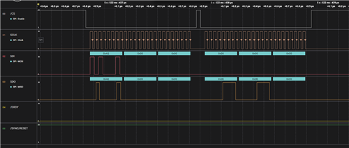
As you can see in the code, I am first trying to just read the status register and obviously, I am expecting the value of 0X500 (default). But I don't get it. In line 924, the 'adcresponse' is 0. I am not sure if the command is sent. I don't have a big logic analyzer, but have a simple DSO. When I debug the code, the SYNC/RESET, CS, all sets well as in the code (I have a toggle reset, hold it high and then I set the CS to low, then invoke the sendCommand, for the command to be sent). When I see the SCLK on the DSO, it remains as a noise with 96mV or something always. I am not sure if the clock is changing and I done see it in the DSO since the freq is high, or the clock doesn't work? I am setting the clock in the code (Line 200 in the above code). Am I missing something?
#ifndef ADS131M0X_H_
#define ADS131M0X_H_
// Standard libraries
#include <assert.h>
//****************************************************************************
//
// Select the device variant to use...
//
//****************************************************************************
#define CHANNEL_COUNT (8) // ADS131M08 -> 8 Channels
#if ((CHANNEL_COUNT < 1) || (CHANNEL_COUNT > 8))
#error Invalid channel count configured in 'ads131m0x.h'.
#endif
//****************************************************************************
//
// Select the desired MODE register settings...
// NOTE: These settings will be enforced and not modifiable during runtime!
//
//****************************************************************************
/* Pick one (and only one) mode to use... */
//#define WORD_LENGTH_16BIT_TRUNCATED
#define WORD_LENGTH_24BIT
//#define WORD_LENGTH_32BIT_SIGN_EXTEND
//#define WORD_LENGTH_32BIT_ZERO_PADDED
/* Enable this define statement to use the DRDY pulse format... */
#define DRDY_FMT_PULSE
/* Enable this define statement to use CRC on DIN... */
//#define ENABLE_CRC_IN
/* Select CRC type */
#define CRC_CCITT
//#define CRC_ANSI
/* Disable assertions when not in the CCS "Debug" configuration */
#ifndef _DEBUG
#define NDEBUG
#endif
//
// Validation
//
// Throw an error if no WORD_LENGTH mode was selected above
#if !defined WORD_LENGTH_16BIT_TRUNCATED && \
!defined WORD_LENGTH_24BIT && \
!defined WORD_LENGTH_32BIT_SIGN_EXTEND && \
!defined WORD_LENGTH_32BIT_ZERO_PADDED
#error Must define at least one WORD_LENGTH mode
#endif
// Throw an error if none or both CRC types are selected
#if !defined CRC_CCITT && !defined CRC_ANSI
#error Must define at least one CRC type
#endif
#if defined CRC_CCITT && defined CRC_ANSI
#error Must define only one CRC type
#endif
//****************************************************************************
//
// Constants
//
//****************************************************************************
#define NUM_REGISTERS ((uint8_t) 64)
//****************************************************************************
//
// SPI command opcodes
//
//****************************************************************************
#define OPCODE_NULL ((uint16_t) 0x0000)
#define OPCODE_RESET ((uint16_t) 0x0011)
#define OPCODE_RREG ((uint16_t) 0xA000)
#define OPCODE_WREG ((uint16_t) 0x6000)
#define OPCODE_STANDBY ((uint16_t) 0x0022)
#define OPCODE_WAKEUP ((uint16_t) 0x0033)
#define OPCODE_LOCK ((uint16_t) 0x0555)
#define OPCODE_UNLOCK ((uint16_t) 0x0655)
//****************************************************************************
//
// Register definitions
//
//****************************************************************************
/* NOTE: Whenever possible, macro names (defined below) were derived from
* datasheet defined names; however, updates to documentation may cause
* mismatches between names defined here in example code from those shown
* in the device datasheet.
*/
/* Register 0x00 (ID) definition - READ ONLY
* -----------------------------------------------------------------------------------------------------------------------------------------------------------------------------------------------------------------
* | Bit 15 | Bit 14 | Bit 13 | Bit 12 | Bit 11 | Bit 10 | Bit 9 | Bit 8 | Bit 7 | Bit 6 | Bit 5 | Bit 4 | Bit 3 | Bit 2 | Bit 1 | Bit 0 |
* -----------------------------------------------------------------------------------------------------------------------------------------------------------------------------------------------------------------
* | RESERVED[3:0] | CHANCNT[3:0] | REVID[7:0] |
* -----------------------------------------------------------------------------------------------------------------------------------------------------------------------------------------------------------------
*/
/* ID register address & default value */
#define ID_ADDRESS ((uint8_t) 0x00)
#define ID_DEFAULT ((uint16_t) 0x2000 | (CHANNEL_COUNT << 8)) // NOTE: May change with future device revisions!
/* RESERVED field mask */
#define ID_RESERVED_MASK ((uint16_t) 0xF000)
/* CHANCNT field mask & values */
#define ID_CHANCNT_MASK ((uint16_t) 0x0F00)
#define ID_CHANCNT_4CH ((uint16_t) 0x0004 << 8)
#define ID_CHANCNT_6CH ((uint16_t) 0x0006 << 8)
#define ID_CHANCNT_8CH ((uint16_t) 0x0008 << 8)
/* REVID field mask & values */
#define ID_REVID_MASK ((uint16_t) 0x00FF)
#define ID_REVID_REVA ((uint16_t) 0x0000 << 0) // DEFAULT
/* Register 0x01 (STATUS) definition - READ ONLY
* -----------------------------------------------------------------------------------------------------------------------------------------------------------------------------------------------------------------
* | Bit 15 | Bit 14 | Bit 13 | Bit 12 | Bit 11 | Bit 10 | Bit 9 | Bit 8 | Bit 7 | Bit 6 | Bit 5 | Bit 4 | Bit 3 | Bit 2 | Bit 1 | Bit 0 |
* -----------------------------------------------------------------------------------------------------------------------------------------------------------------------------------------------------------------
* | LOCK | F_RESYNC | REG_MAP | CRC_ERR | CRC_TYPE | RESET | WLENGTH[1:0] | DRDY7 | DRDY6 | DRDY5 | DRDY4 | DRDY3 | DRDY2 | DRDY1 | DRDY0 |
* -----------------------------------------------------------------------------------------------------------------------------------------------------------------------------------------------------------------
* NOTE 1: Bits 0 through 7 are hardware controlled. Reading these values multiple times may return different results.
* NOTE 2: Bits 0 through 4 are RESERVED on the ADS131M04. These bits will always read 0.
*/
/* STATUS register address & default value */
#define STATUS_ADDRESS ((uint8_t) 0x01)
#define STATUS_DEFAULT ((uint16_t) 0x0500)
/* LOCK field mask & values */
#define STATUS_LOCK_MASK ((uint16_t) 0x8000)
#define STATUS_LOCK_UNLOCKED ((uint16_t) 0x0000 << 15) // DEFAULT
#define STATUS_LOCK_LOCKED ((uint16_t) 0x0001 << 15)
/* F_RESYNC field mask & values */
#define STATUS_F_RESYNC_MASK ((uint16_t) 0x4000)
#define STATUS_F_RESYNC_NO_FAULT ((uint16_t) 0x0000 << 14) // DEFAULT
#define STATUS_F_RESYNC_FAULT ((uint16_t) 0x0001 << 14)
/* REG_MAP field mask & values */
#define STATUS_REG_MAP_MASK ((uint16_t) 0x2000)
#define STATUS_REG_MAP_NO_CHANGE_CRC ((uint16_t) 0x0000 << 13) // DEFAULT
#define STATUS_REG_MAP_CHANGED_CRC ((uint16_t) 0x0001 << 13)
/* CRC_ERR field mask & values */
#define STATUS_CRC_ERR_MASK ((uint16_t) 0x1000)
#define STATUS_CRC_ERR_NO_CRC_ERROR ((uint16_t) 0x0000 << 12) // DEFAULT
#define STATUS_CRC_ERR_INPUT_CRC_ERROR ((uint16_t) 0x0001 << 12)
/* CRC_TYPE field mask & values */
#define STATUS_CRC_TYPE_MASK ((uint16_t) 0x0800)
#define STATUS_CRC_TYPE_16BIT_CCITT ((uint16_t) 0x0000 << 11) // DEFAULT
#define STATUS_CRC_TYPE_16BIT_ANSI ((uint16_t) 0x0001 << 11)
/* RESET field mask & values */
#define STATUS_RESET_MASK ((uint16_t) 0x0400)
#define STATUS_RESET_NO_RESET ((uint16_t) 0x0000 << 10)
#define STATUS_RESET_RESET_OCCURRED ((uint16_t) 0x0001 << 10) // DEFAULT
/* WLENGTH field mask & values */
#define STATUS_WLENGTH_MASK ((uint16_t) 0x0300)
#define STATUS_WLENGTH_16BIT ((uint16_t) 0x0000 << 8)
#define STATUS_WLENGTH_24BIT ((uint16_t) 0x0001 << 8) // DEFAULT
#define STATUS_WLENGTH_32BIT_LSB_ZEROES ((uint16_t) 0x0002 << 8)
#define STATUS_WLENGTH_32BIT_MSB_SIGN_EXT ((uint16_t) 0x0003 << 8)
#if (CHANNEL_COUNT > 7)
/* DRDY7 field mask & values */
#define STATUS_DRDY7_MASK ((uint16_t) 0x0080)
#define STATUS_DRDY7_NO_NEW_DATA ((uint16_t) 0x0000 << 7)
#define STATUS_DRDY7_NEW_DATA ((uint16_t) 0x0001 << 7)
#endif
#if (CHANNEL_COUNT > 6)
/* DRDY6 field mask & values */
#define STATUS_DRDY6_MASK ((uint16_t) 0x0040)
#define STATUS_DRDY6_NO_NEW_DATA ((uint16_t) 0x0000 << 6)
#define STATUS_DRDY6_NEW_DATA ((uint16_t) 0x0001 << 6)
#endif
#if (CHANNEL_COUNT > 5)
/* DRDY5 field mask & values */
#define STATUS_DRDY5_MASK ((uint16_t) 0x0020)
#define STATUS_DRDY5_NO_NEW_DATA ((uint16_t) 0x0000 << 5)
#define STATUS_DRDY5_NEW_DATA ((uint16_t) 0x0001 << 5)
#endif
#if (CHANNEL_COUNT > 4)
/* DRDY4 field mask & values */
#define STATUS_DRDY4_MASK ((uint16_t) 0x0010)
#define STATUS_DRDY4_NO_NEW_DATA ((uint16_t) 0x0000 << 4)
#define STATUS_DRDY4_NEW_DATA ((uint16_t) 0x0001 << 4)
#endif
#if (CHANNEL_COUNT > 3)
/* DRDY3 field mask & values */
#define STATUS_DRDY3_MASK ((uint16_t) 0x0008)
#define STATUS_DRDY3_NO_NEW_DATA ((uint16_t) 0x0000 << 3)
#define STATUS_DRDY3_NEW_DATA ((uint16_t) 0x0001 << 3)
#endif
#if (CHANNEL_COUNT > 2)
/* DRDY2 field mask & values */
#define STATUS_DRDY2_MASK ((uint16_t) 0x0004)
#define STATUS_DRDY2_NO_NEW_DATA ((uint16_t) 0x0000 << 2)
#define STATUS_DRDY2_NEW_DATA ((uint16_t) 0x0001 << 2)
#endif
#if (CHANNEL_COUNT > 1)
/* DRDY1 field mask & values */
#define STATUS_DRDY1_MASK ((uint16_t) 0x0002)
#define STATUS_DRDY1_NO_NEW_DATA ((uint16_t) 0x0000 << 1)
#define STATUS_DRDY1_NEW_DATA ((uint16_t) 0x0001 << 1)
#endif
/* DRDY0 field mask & values */
#define STATUS_DRDY0_MASK ((uint16_t) 0x0001)
#define STATUS_DRDY0_NO_NEW_DATA ((uint16_t) 0x0000 << 0)
#define STATUS_DRDY0_NEW_DATA ((uint16_t) 0x0001 << 0)
/* Register 0x02 (MODE) definition
* -----------------------------------------------------------------------------------------------------------------------------------------------------------------------------------------------------------------
* | Bit 15 | Bit 14 | Bit 13 | Bit 12 | Bit 11 | Bit 10 | Bit 9 | Bit 8 | Bit 7 | Bit 6 | Bit 5 | Bit 4 | Bit 3 | Bit 2 | Bit 1 | Bit 0 |
* -----------------------------------------------------------------------------------------------------------------------------------------------------------------------------------------------------------------
* | RESERVED0[1:0] | REG_CRC_EN | RX_CRC_EN | CRC_TYPE | RESET | WLENGTH[1:0] | RESERVED1[2:0] | TIMEOUT | DRDY_SEL[1:0] | DRDY_HiZ | DRDY_FMT |
* -----------------------------------------------------------------------------------------------------------------------------------------------------------------------------------------------------------------
*/
/* MODE register address & default value */
#define MODE_ADDRESS ((uint8_t) 0x02)
#define MODE_DEFAULT ((uint16_t) 0x0510)
/* RESERVED0 field mask */
#define MODE_RESERVED0_MASK ((uint16_t) 0xC000)
/* REG_CRC_EN field mask & values */
#define MODE_REG_CRC_EN_MASK ((uint16_t) 0x2000)
#define MODE_REG_CRC_EN_DISABLED ((uint16_t) 0x0000 << 13) // DEFAULT
#define MODE_REG_CRC_EN_ENABLED ((uint16_t) 0x0001 << 13)
/* RX_CRC_EN field mask & values */
#define MODE_RX_CRC_EN_MASK ((uint16_t) 0x1000)
#define MODE_RX_CRC_EN_DISABLED ((uint16_t) 0x0000 << 12) // DEFAULT
#define MODE_RX_CRC_EN_ENABLED ((uint16_t) 0x0001 << 12)
/* CRC_TYPE field mask & values */
#define MODE_CRC_TYPE_MASK ((uint16_t) 0x0800)
#define MODE_CRC_TYPE_16BIT_CCITT ((uint16_t) 0x0000 << 11) // DEFAULT
#define MODE_CRC_TYPE_16BIT_ANSI ((uint16_t) 0x0001 << 11)
/* RESET field mask & values */
#define MODE_RESET_MASK ((uint16_t) 0x0400)
#define MODE_RESET_NO_RESET ((uint16_t) 0x0000 << 10)
#define MODE_RESET_RESET_OCCURRED ((uint16_t) 0x0001 << 10) // DEFAULT
/* WLENGTH field mask & values */
#define MODE_WLENGTH_MASK ((uint16_t) 0x0300)
#define MODE_WLENGTH_16BIT ((uint16_t) 0x0000 << 8)
#define MODE_WLENGTH_24BIT ((uint16_t) 0x0001 << 8)
#define MODE_WLENGTH_32BIT_LSB_ZEROES ((uint16_t) 0x0002 << 8)
#define MODE_WLENGTH_32BIT_MSB_SIGN_EXT ((uint16_t) 0x0003 << 8)
/* RESERVED1 field mask */
#define MODE_RESERVED1_MASK ((uint16_t) 0x00E0)
/* TIMEOUT field mask & values */
#define MODE_TIMEOUT_MASK ((uint16_t) 0x0010)
#define MODE_TIMEOUT_DISABLED ((uint16_t) 0x0000 << 4)
#define MODE_TIMEOUT_ENABLED ((uint16_t) 0x0001 << 4) // DEFAULT
/* DRDY_SEL field mask & values */
#define MODE_DRDY_SEL_MASK ((uint16_t) 0x000C)
#define MODE_DRDY_SEL_MOST_LAGGING ((uint16_t) 0x0000 << 2) // DEFAULT
#define MODE_DRDY_SEL_LOGIC_OR ((uint16_t) 0x0001 << 2)
#define MODE_DRDY_SEL_MOST_LEADING ((uint16_t) 0x0002 << 2) // Alternative value: ((uint16_t) 0x0003 << 2)
/* DRDY_HiZ field mask & values */
#define MODE_DRDY_HiZ_MASK ((uint16_t) 0x0002)
#define MODE_DRDY_HiZ_LOGIC_HIGH ((uint16_t) 0x0000 << 1) // DEFAULT
#define MODE_DRDY_HiZ_HIGH_IMPEDANCE ((uint16_t) 0x0001 << 1)
/* DRDY_FMT field mask & values */
#define MODE_DRDY_FMT_MASK ((uint16_t) 0x0001)
#define MODE_DRDY_FMT_LOGIC_LOW ((uint16_t) 0x0000 << 0) // DEFAULT
#define MODE_DRDY_FMT_NEG_PULSE_FIXED_WIDTH ((uint16_t) 0x0001 << 0)
/* Register 0x03 (CLOCK) definition
* -----------------------------------------------------------------------------------------------------------------------------------------------------------------------------------------------------------------
* | Bit 15 | Bit 14 | Bit 13 | Bit 12 | Bit 11 | Bit 10 | Bit 9 | Bit 8 | Bit 7 | Bit 6 | Bit 5 | Bit 4 | Bit 3 | Bit 2 | Bit 1 | Bit 0 |
* -----------------------------------------------------------------------------------------------------------------------------------------------------------------------------------------------------------------
* | CH7_EN | CH6_EN | CH5_EN | CH4_EN | CH3_EN | CH2_EN | CH1_EN | CH0_EN | RESERVED[2:0] | OSR[2:0] | PWR[1:0] |
* -----------------------------------------------------------------------------------------------------------------------------------------------------------------------------------------------------------------
* NOTE 1: Bits 12 through 15 are RESERVED on the ADS131M04.
*/
/* CLOCK register address & default value */
#define CLOCK_ADDRESS ((uint8_t) 0x03)
#if (CHANNEL_COUNT == 8)
#define CLOCK_DEFAULT ((uint16_t) 0xFF0E)
#endif
#if (CHANNEL_COUNT == 7)
#define CLOCK_DEFAULT ((uint16_t) 0x7F0E)
#endif
#if (CHANNEL_COUNT == 6)
#define CLOCK_DEFAULT ((uint16_t) 0x3F0E)
#endif
#if (CHANNEL_COUNT == 5)
#define CLOCK_DEFAULT ((uint16_t) 0x1F0E)
#endif
#if (CHANNEL_COUNT == 4)
#define CLOCK_DEFAULT ((uint16_t) 0x0F0E)
#endif
#if (CHANNEL_COUNT == 3)
#define CLOCK_DEFAULT ((uint16_t) 0x070E)
#endif
#if (CHANNEL_COUNT == 2)
#define CLOCK_DEFAULT ((uint16_t) 0x030E)
#endif
#if (CHANNEL_COUNT == 1)
#define CLOCK_DEFAULT ((uint16_t) 0x010E)
#endif
#if (CHANNEL_COUNT > 7)
/* CH7_EN field mask & values */
#define CLOCK_CH7_EN_MASK ((uint16_t) 0x8000)
#define CLOCK_CH7_EN_DISABLED ((uint16_t) 0x0000 << 15)
#define CLOCK_CH7_EN_ENABLED ((uint16_t) 0x0001 << 15)
#endif
#if (CHANNEL_COUNT > 6)
/* CH6_EN field mask & values */
#define CLOCK_CH6_EN_MASK ((uint16_t) 0x4000)
#define CLOCK_CH6_EN_DISABLED ((uint16_t) 0x0000 << 14)
#define CLOCK_CH6_EN_ENABLED ((uint16_t) 0x0001 << 14)
#endif
#if (CHANNEL_COUNT > 5)
/* CH5_EN field mask & values */
#define CLOCK_CH5_EN_MASK ((uint16_t) 0x2000)
#define CLOCK_CH5_EN_DISABLED ((uint16_t) 0x0000 << 13)
#define CLOCK_CH5_EN_ENABLED ((uint16_t) 0x0001 << 13)
#endif
#if (CHANNEL_COUNT > 4)
/* CH4_EN field mask & values */
#define CLOCK_CH4_EN_MASK ((uint16_t) 0x1000)
#define CLOCK_CH4_EN_DISABLED ((uint16_t) 0x0000 << 12)
#define CLOCK_CH4_EN_ENABLED ((uint16_t) 0x0001 << 12)
#endif
#if (CHANNEL_COUNT > 3)
/* CH3_EN field mask & values */
#define CLOCK_CH3_EN_MASK ((uint16_t) 0x0800)
#define CLOCK_CH3_EN_DISABLED ((uint16_t) 0x0000 << 11)
#define CLOCK_CH3_EN_ENABLED ((uint16_t) 0x0001 << 11)
#endif
#if (CHANNEL_COUNT > 2)
/* CH2_EN field mask & values */
#define CLOCK_CH2_EN_MASK ((uint16_t) 0x0400)
#define CLOCK_CH2_EN_DISABLED ((uint16_t) 0x0000 << 10)
#define CLOCK_CH2_EN_ENABLED ((uint16_t) 0x0001 << 10)
#endif
#if (CHANNEL_COUNT > 1)
/* CH1_EN field mask & values */
#define CLOCK_CH1_EN_MASK ((uint16_t) 0x0200)
#define CLOCK_CH1_EN_DISABLED ((uint16_t) 0x0000 << 9)
#define CLOCK_CH1_EN_ENABLED ((uint16_t) 0x0001 << 9)
#endif
/* CH0_EN field mask & values */
#define CLOCK_CH0_EN_MASK ((uint16_t) 0x0100)
#define CLOCK_CH0_EN_DISABLED ((uint16_t) 0x0000 << 8)
#define CLOCK_CH0_EN_ENABLED ((uint16_t) 0x0001 << 8) // DEFAULT
/* RESERVED1 field mask */
#define CLOCK_RESERVED_MASK ((uint16_t) 0x00E0)
/* OSR field mask & values */
#define CLOCK_OSR_MASK ((uint16_t) 0x001C)
#define CLOCK_OSR_128 ((uint16_t) 0x0000 << 2)
#define CLOCK_OSR_256 ((uint16_t) 0x0001 << 2)
#define CLOCK_OSR_512 ((uint16_t) 0x0002 << 2)
#define CLOCK_OSR_1024 ((uint16_t) 0x0003 << 2) // DEFAULT
#define CLOCK_OSR_2048 ((uint16_t) 0x0004 << 2)
#define CLOCK_OSR_4096 ((uint16_t) 0x0005 << 2)
#define CLOCK_OSR_8192 ((uint16_t) 0x0006 << 2)
#define CLOCK_OSR_16384 ((uint16_t) 0x0007 << 2)
/* PWR field mask & values */
#define CLOCK_PWR_MASK ((uint16_t) 0x0003)
#define CLOCK_PWR_VLP ((uint16_t) 0x0000 << 0)
#define CLOCK_PWR_LP ((uint16_t) 0x0001 << 0)
#define CLOCK_PWR_HR ((uint16_t) 0x0002 << 0) // DEFAULT, Alternative value: ((uint16_t) 0x0003 << 2)
/* Register 0x04 (GAIN1) definition
* -----------------------------------------------------------------------------------------------------------------------------------------------------------------------------------------------------------------
* | Bit 15 | Bit 14 | Bit 13 | Bit 12 | Bit 11 | Bit 10 | Bit 9 | Bit 8 | Bit 7 | Bit 6 | Bit 5 | Bit 4 | Bit 3 | Bit 2 | Bit 1 | Bit 0 |
* -----------------------------------------------------------------------------------------------------------------------------------------------------------------------------------------------------------------
* | RESERVED0 | PGAGAIN3[2:0] | RESERVED1 | PGAGAIN2[2:0] | RESERVED2 | PGAGAIN1[2:0] | RESERVED3 | PGAGAIN0[2:0] |
* -----------------------------------------------------------------------------------------------------------------------------------------------------------------------------------------------------------------
*/
/* GAIN1 register address & default value */
#define GAIN1_ADDRESS ((uint8_t) 0x04)
#define GAIN1_DEFAULT ((uint16_t) 0x0000)
/* RESERVED0 field mask & values */
#define GAIN1_RESERVED0_MASK ((uint16_t) 0x8000)
/* PGAGAIN3 field mask & values */
#define GAIN1_PGAGAIN3_MASK ((uint16_t) 0x7000)
#define GAIN1_PGAGAIN3_1 ((uint16_t) 0x0000 << 12) // DEFAULT
#define GAIN1_PGAGAIN3_2 ((uint16_t) 0x0001 << 12)
#define GAIN1_PGAGAIN3_4 ((uint16_t) 0x0002 << 12)
#define GAIN1_PGAGAIN3_8 ((uint16_t) 0x0003 << 12)
#define GAIN1_PGAGAIN3_16 ((uint16_t) 0x0004 << 12)
#define GAIN1_PGAGAIN3_32 ((uint16_t) 0x0005 << 12)
#define GAIN1_PGAGAIN3_64 ((uint16_t) 0x0006 << 12)
#define GAIN1_PGAGAIN3_128 ((uint16_t) 0x0007 << 12)
/* RESERVED1 field mask & values */
#define GAIN1_RESERVED1_MASK ((uint16_t) 0x0800)
/* PGAGAIN2 field mask & values */
#define GAIN1_PGAGAIN2_MASK ((uint16_t) 0x0700)
#define GAIN1_PGAGAIN2_1 ((uint16_t) 0x0000 << 8) // DEFAULT
#define GAIN1_PGAGAIN2_2 ((uint16_t) 0x0001 << 8)
#define GAIN1_PGAGAIN2_4 ((uint16_t) 0x0002 << 8)
#define GAIN1_PGAGAIN2_8 ((uint16_t) 0x0003 << 8)
#define GAIN1_PGAGAIN2_16 ((uint16_t) 0x0004 << 8)
#define GAIN1_PGAGAIN2_32 ((uint16_t) 0x0005 << 8)
#define GAIN1_PGAGAIN2_64 ((uint16_t) 0x0006 << 8)
#define GAIN1_PGAGAIN2_128 ((uint16_t) 0x0007 << 8)
/* RESERVED2 field mask & values */
#define GAIN1_RESERVED2_MASK ((uint16_t) 0x0080)
/* PGAGAIN1 field mask & values */
#define GAIN1_PGAGAIN1_MASK ((uint16_t) 0x0070)
#define GAIN1_PGAGAIN1_1 ((uint16_t) 0x0000 << 4) // DEFAULT
#define GAIN1_PGAGAIN1_2 ((uint16_t) 0x0001 << 4)
#define GAIN1_PGAGAIN1_4 ((uint16_t) 0x0002 << 4)
#define GAIN1_PGAGAIN1_8 ((uint16_t) 0x0003 << 4)
#define GAIN1_PGAGAIN1_16 ((uint16_t) 0x0004 << 4)
#define GAIN1_PGAGAIN1_32 ((uint16_t) 0x0005 << 4)
#define GAIN1_PGAGAIN1_64 ((uint16_t) 0x0006 << 4)
#define GAIN1_PGAGAIN1_128 ((uint16_t) 0x0007 << 4)
/* RESERVED3 field mask & values */
#define GAIN1_RESERVED3_MASK ((uint16_t) 0x0008)
/* PGAGAIN0 field mask & values */
#define GAIN1_PGAGAIN0_MASK ((uint16_t) 0x0007)
#define GAIN1_PGAGAIN0_1 ((uint16_t) 0x0000 << 0) // DEFAULT
#define GAIN1_PGAGAIN0_2 ((uint16_t) 0x0001 << 0)
#define GAIN1_PGAGAIN0_4 ((uint16_t) 0x0002 << 0)
#define GAIN1_PGAGAIN0_8 ((uint16_t) 0x0003 << 0)
#define GAIN1_PGAGAIN0_16 ((uint16_t) 0x0004 << 0)
#define GAIN1_PGAGAIN0_32 ((uint16_t) 0x0005 << 0)
#define GAIN1_PGAGAIN0_64 ((uint16_t) 0x0006 << 0)
#define GAIN1_PGAGAIN0_128 ((uint16_t) 0x0007 << 0)
/* Register 0x05 (GAIN2) definition
* -----------------------------------------------------------------------------------------------------------------------------------------------------------------------------------------------------------------
* | Bit 15 | Bit 14 | Bit 13 | Bit 12 | Bit 11 | Bit 10 | Bit 9 | Bit 8 | Bit 7 | Bit 6 | Bit 5 | Bit 4 | Bit 3 | Bit 2 | Bit 1 | Bit 0 |
* -----------------------------------------------------------------------------------------------------------------------------------------------------------------------------------------------------------------
* | RESERVED0 | PGAGAIN7[2:0] | RESERVED1 | PGAGAIN6[2:0] | RESERVED2 | PGAGAIN5[2:0] | RESERVED3 | PGAGAIN4[2:0] |
* -----------------------------------------------------------------------------------------------------------------------------------------------------------------------------------------------------------------
* NOTE 1: This register is RESERVED on the ADS131M04. Only write 0x0000 to this register.
*/
/* GAIN2 register address & default value */
#define GAIN2_ADDRESS ((uint8_t) 0x05)
#define GAIN2_DEFAULT ((uint16_t) 0x0000)
#if (CHANNEL_COUNT > 4)
/* RESERVED0 field mask & values */
#define GAIN2_RESERVED0_MASK ((uint16_t) 0x8000)
/* PGAGAIN7 field mask & values */
#define GAIN2_PGAGAIN7_MASK ((uint16_t) 0x7000)
#define GAIN2_PGAGAIN7_1 ((uint16_t) 0x0000 << 12) // DEFAULT
#define GAIN2_PGAGAIN7_2 ((uint16_t) 0x0001 << 12)
#define GAIN2_PGAGAIN7_4 ((uint16_t) 0x0002 << 12)
#define GAIN2_PGAGAIN7_8 ((uint16_t) 0x0003 << 12)
#define GAIN2_PGAGAIN7_16 ((uint16_t) 0x0004 << 12)
#define GAIN2_PGAGAIN7_32 ((uint16_t) 0x0005 << 12)
#define GAIN2_PGAGAIN7_64 ((uint16_t) 0x0006 << 12)
#define GAIN2_PGAGAIN7_128 ((uint16_t) 0x0007 << 12)
/* RESERVED1 field mask & values */
#define GAIN2_RESERVED1_MASK ((uint16_t) 0x0800)
/* PGAGAIN6 field mask & values */
#define GAIN2_PGAGAIN6_MASK ((uint16_t) 0x0700)
#define GAIN2_PGAGAIN6_1 ((uint16_t) 0x0000 << 8) // DEFAULT
#define GAIN2_PGAGAIN6_2 ((uint16_t) 0x0001 << 8)
#define GAIN2_PGAGAIN6_4 ((uint16_t) 0x0002 << 8)
#define GAIN2_PGAGAIN6_8 ((uint16_t) 0x0003 << 8)
#define GAIN2_PGAGAIN6_16 ((uint16_t) 0x0004 << 8)
#define GAIN2_PGAGAIN6_32 ((uint16_t) 0x0005 << 8)
#define GAIN2_PGAGAIN6_64 ((uint16_t) 0x0006 << 8)
#define GAIN2_PGAGAIN6_128 ((uint16_t) 0x0007 << 8)
/* RESERVED2 field mask & values */
#define GAIN2_RESERVED2_MASK ((uint16_t) 0x0080)
/* PGAGAIN5 field mask & values */
#define GAIN2_PGAGAIN5_MASK ((uint16_t) 0x0070)
#define GAIN2_PGAGAIN5_1 ((uint16_t) 0x0000 << 4) // DEFAULT
#define GAIN2_PGAGAIN5_2 ((uint16_t) 0x0001 << 4)
#define GAIN2_PGAGAIN5_4 ((uint16_t) 0x0002 << 4)
#define GAIN2_PGAGAIN5_8 ((uint16_t) 0x0003 << 4)
#define GAIN2_PGAGAIN5_16 ((uint16_t) 0x0004 << 4)
#define GAIN2_PGAGAIN5_32 ((uint16_t) 0x0005 << 4)
#define GAIN2_PGAGAIN5_64 ((uint16_t) 0x0006 << 4)
#define GAIN2_PGAGAIN5_128 ((uint16_t) 0x0007 << 4)
/* RESERVED3 field mask & values */
#define GAIN2_RESERVED3_MASK ((uint16_t) 0x0008)
/* PGAGAIN4 field mask & values */
#define GAIN2_PGAGAIN4_MASK ((uint16_t) 0x0007)
#define GAIN2_PGAGAIN4_1 ((uint16_t) 0x0000 << 0) // DEFAULT
#define GAIN2_PGAGAIN4_2 ((uint16_t) 0x0001 << 0)
#define GAIN2_PGAGAIN4_4 ((uint16_t) 0x0002 << 0)
#define GAIN2_PGAGAIN4_8 ((uint16_t) 0x0003 << 0)
#define GAIN2_PGAGAIN4_16 ((uint16_t) 0x0004 << 0)
#define GAIN2_PGAGAIN4_32 ((uint16_t) 0x0005 << 0)
#define GAIN2_PGAGAIN4_64 ((uint16_t) 0x0006 << 0)
#define GAIN2_PGAGAIN4_128 ((uint16_t) 0x0007 << 0)
#endif
/* Register 0x06 (CFG) definition
* -----------------------------------------------------------------------------------------------------------------------------------------------------------------------------------------------------------------
* | Bit 15 | Bit 14 | Bit 13 | Bit 12 | Bit 11 | Bit 10 | Bit 9 | Bit 8 | Bit 7 | Bit 6 | Bit 5 | Bit 4 | Bit 3 | Bit 2 | Bit 1 | Bit 0 |
* -----------------------------------------------------------------------------------------------------------------------------------------------------------------------------------------------------------------
* | RESERVED0[2:0] | GC_DLY[3:0] | GC_EN | CD_ALLCH | CD_NUM[2:0] | CD_LEN[2:0] | CD_EN |
* -----------------------------------------------------------------------------------------------------------------------------------------------------------------------------------------------------------------
*/
/* CFG register address & default value */
#define CFG_ADDRESS ((uint8_t) 0x06)
#define CFG_DEFAULT ((uint16_t) 0x0600)
/* RESERVED0 field mask & values */
#define CFG_RESERVED0_MASK ((uint16_t) 0xE000)
/* GC_DLY field mask & values */
#define CFG_GC_DLY_MASK ((uint16_t) 0x1E00)
#define CFG_GC_DLY_2 ((uint16_t) 0x0000 << 9)
#define CFG_GC_DLY_4 ((uint16_t) 0x0001 << 9)
#define CFG_GC_DLY_8 ((uint16_t) 0x0002 << 9)
#define CFG_GC_DLY_16 ((uint16_t) 0x0003 << 9) // DEFAULT
#define CFG_GC_DLY_32 ((uint16_t) 0x0004 << 9)
#define CFG_GC_DLY_64 ((uint16_t) 0x0005 << 9)
#define CFG_GC_DLY_128 ((uint16_t) 0x0006 << 9)
#define CFG_GC_DLY_256 ((uint16_t) 0x0007 << 9)
#define CFG_GC_DLY_512 ((uint16_t) 0x0008 << 9)
#define CFG_GC_DLY_1024 ((uint16_t) 0x0009 << 9)
#define CFG_GC_DLY_2048 ((uint16_t) 0x000A << 9)
#define CFG_GC_DLY_4096 ((uint16_t) 0x000B << 9)
#define CFG_GC_DLY_8192 ((uint16_t) 0x000C << 9)
#define CFG_GC_DLY_16484 ((uint16_t) 0x000D << 9)
#define CFG_GC_DLY_32768 ((uint16_t) 0x000E << 9)
#define CFG_GC_DLY_65536 ((uint16_t) 0x000F << 9)
/* GC_EN field mask & values */
#define CFG_GC_EN_MASK ((uint16_t) 0x0100)
#define CFG_GC_EN_DISABLED ((uint16_t) 0x0000 << 8) // DEFAULT
#define CFG_GC_EN_ENABLED ((uint16_t) 0x0001 << 8)
/* CD_ALLCH field mask & values */
#define CFG_CD_ALLCH_MASK ((uint16_t) 0x0080)
#define CFG_CD_ALLCH_ANY_CHANNEL ((uint16_t) 0x0000 << 7) // DEFAULT
#define CFG_CD_ALLCH_ALL_CHANNELS ((uint16_t) 0x0001 << 7)
/* CD_NUM field mask & values */
#define CFG_CD_NUM_MASK ((uint16_t) 0x0070)
#define CFG_CD_NUM_1 ((uint16_t) 0x0000 << 4) // DEFAULT
#define CFG_CD_NUM_2 ((uint16_t) 0x0001 << 4)
#define CFG_CD_NUM_4 ((uint16_t) 0x0002 << 4)
#define CFG_CD_NUM_8 ((uint16_t) 0x0003 << 4)
#define CFG_CD_NUM_16 ((uint16_t) 0x0004 << 4)
#define CFG_CD_NUM_32 ((uint16_t) 0x0005 << 4)
#define CFG_CD_NUM_64 ((uint16_t) 0x0006 << 4)
#define CFG_CD_NUM_128 ((uint16_t) 0x0007 << 4)
/* CD_LEN field mask & values */
#define CFG_CD_LEN_MASK ((uint16_t) 0x000E)
#define CFG_CD_LEN_128 ((uint16_t) 0x0000 << 1) // DEFAULT
#define CFG_CD_LEN_256 ((uint16_t) 0x0001 << 1)
#define CFG_CD_LEN_512 ((uint16_t) 0x0002 << 1)
#define CFG_CD_LEN_768 ((uint16_t) 0x0003 << 1)
#define CFG_CD_LEN_1280 ((uint16_t) 0x0004 << 1)
#define CFG_CD_LEN_1792 ((uint16_t) 0x0005 << 1)
#define CFG_CD_LEN_2560 ((uint16_t) 0x0006 << 1)
#define CFG_CD_LEN_3584 ((uint16_t) 0x0007 << 1)
/* CD_EN field mask & values */
#define CFG_CD_EN_MASK ((uint16_t) 0x0001)
#define CFG_CD_EN_DISABLED ((uint16_t) 0x0000 << 0) // DEFAULT
#define CFG_CD_EN_ENABLED ((uint16_t) 0x0001 << 0)
/* Register 0x07 (THRSHLD_MSB) definition
* -----------------------------------------------------------------------------------------------------------------------------------------------------------------------------------------------------------------
* | Bit 15 | Bit 14 | Bit 13 | Bit 12 | Bit 11 | Bit 10 | Bit 9 | Bit 8 | Bit 7 | Bit 6 | Bit 5 | Bit 4 | Bit 3 | Bit 2 | Bit 1 | Bit 0 |
* -----------------------------------------------------------------------------------------------------------------------------------------------------------------------------------------------------------------
* | CD_TH_MSB[15:0] |
* -----------------------------------------------------------------------------------------------------------------------------------------------------------------------------------------------------------------
*/
/* THRSHLD_MSB register address & default value */
#define THRSHLD_MSB_ADDRESS ((uint8_t) 0x07)
#define THRSHLD_MSB_DEFAULT ((uint16_t) 0x0000)
/* CD_TH_MSB field mask & values */
#define THRSHLD_MSB_CD_TH_MSB_MASK ((uint16_t) 0xFFFF)
/* Register 0x08 (THRSHLD_LSB) definition
* -----------------------------------------------------------------------------------------------------------------------------------------------------------------------------------------------------------------
* | Bit 15 | Bit 14 | Bit 13 | Bit 12 | Bit 11 | Bit 10 | Bit 9 | Bit 8 | Bit 7 | Bit 6 | Bit 5 | Bit 4 | Bit 3 | Bit 2 | Bit 1 | Bit 0 |
* -----------------------------------------------------------------------------------------------------------------------------------------------------------------------------------------------------------------
* | CD_TH_LSB[7:0] | RESERVED0[7:0] |
* -----------------------------------------------------------------------------------------------------------------------------------------------------------------------------------------------------------------
*/
/* THRSHLD_LSB register address & default value */
#define THRSHLD_LSB_ADDRESS ((uint8_t) 0x08)
#define THRSHLD_LSB_DEFAULT ((uint16_t) 0x0000)
/* CD_TH_LSB field mask & values */
#define THRSHLD_LSB_CD_TH_LSB_MASK ((uint16_t) 0xFF00)
/* RESERVED0 field mask & values */
#define THRSHLD_LSB_RESERVED0_MASK ((uint16_t) 0x00FF)
/* Register 0x09 (CH0_CFG) definition
* -----------------------------------------------------------------------------------------------------------------------------------------------------------------------------------------------------------------
* | Bit 15 | Bit 14 | Bit 13 | Bit 12 | Bit 11 | Bit 10 | Bit 9 | Bit 8 | Bit 7 | Bit 6 | Bit 5 | Bit 4 | Bit 3 | Bit 2 | Bit 1 | Bit 0 |
* -----------------------------------------------------------------------------------------------------------------------------------------------------------------------------------------------------------------
* | PHASE0[9:0] | RESERVED0[3:0] | MUX0[1:0] |
* -----------------------------------------------------------------------------------------------------------------------------------------------------------------------------------------------------------------
*/
/* CH0_CFG register address & default value */
#define CH0_CFG_ADDRESS ((uint8_t) 0x09)
#define CH0_CFG_DEFAULT ((uint16_t) 0x0000)
/* PHASE0 field mask & values */
#define CH0_CFG_PHASE0_MASK ((uint16_t) 0xFFC0)
/* RESERVED0 field mask & values */
#define CH0_CFG_RESERVED0_MASK ((uint16_t) 0x003C)
/* MUX0 field mask & values */
#define CH0_CFG_MUX0_MASK ((uint16_t) 0x0003)
#define CH0_CFG_MUX0_AIN0P_AIN0N ((uint16_t) 0x0000 << 0) // DEFAULT
#define CH0_CFG_MUX0_ADC_INPUT_SHORT ((uint16_t) 0x0001 << 0)
#define CH0_CFG_MUX0_DC_DIAGNOSTIC ((uint16_t) 0x0002 << 0)
#define CH0_CFG_MUX0_AC_DIAGNOSTIC ((uint16_t) 0x0003 << 0)
/* Register 0x0A (CH0_OCAL_MSB) definition
* -----------------------------------------------------------------------------------------------------------------------------------------------------------------------------------------------------------------
* | Bit 15 | Bit 14 | Bit 13 | Bit 12 | Bit 11 | Bit 10 | Bit 9 | Bit 8 | Bit 7 | Bit 6 | Bit 5 | Bit 4 | Bit 3 | Bit 2 | Bit 1 | Bit 0 |
* -----------------------------------------------------------------------------------------------------------------------------------------------------------------------------------------------------------------
* | OCAL0_MSB[15:0] |
* -----------------------------------------------------------------------------------------------------------------------------------------------------------------------------------------------------------------
*/
/* CH0_OCAL_MSB register address & default value */
#define CH0_OCAL_MSB_ADDRESS ((uint8_t) 0x0A)
#define CH0_OCAL_MSB_DEFAULT ((uint16_t) 0x0000)
/* OCAL0_MSB field mask & values */
#define CH0_OCAL_MSB_OCAL0_MSB_MASK ((uint16_t) 0xFFFF)
/* Register 0x0B (CH0_OCAL_LSB) definition
* -----------------------------------------------------------------------------------------------------------------------------------------------------------------------------------------------------------------
* | Bit 15 | Bit 14 | Bit 13 | Bit 12 | Bit 11 | Bit 10 | Bit 9 | Bit 8 | Bit 7 | Bit 6 | Bit 5 | Bit 4 | Bit 3 | Bit 2 | Bit 1 | Bit 0 |
* -----------------------------------------------------------------------------------------------------------------------------------------------------------------------------------------------------------------
* | OCAL0_LSB[7:0] | RESERVED0[7:0] |
* -----------------------------------------------------------------------------------------------------------------------------------------------------------------------------------------------------------------
*/
/* CH0_OCAL_LSB register address & default value */
#define CH0_OCAL_LSB_ADDRESS ((uint8_t) 0x0B)
#define CH0_OCAL_LSB_DEFAULT ((uint16_t) 0x0000)
/* OCAL0_LSB field mask & values */
#define CH0_OCAL_LSB_OCAL0_LSB_MASK ((uint16_t) 0xFF00)
/* RESERVED0 field mask & values */
#define CH0_OCAL_LSB_RESERVED0_MASK ((uint16_t) 0x00FF)
/* Register 0x0C (CH0_GCAL_MSB) definition
* -----------------------------------------------------------------------------------------------------------------------------------------------------------------------------------------------------------------
* | Bit 15 | Bit 14 | Bit 13 | Bit 12 | Bit 11 | Bit 10 | Bit 9 | Bit 8 | Bit 7 | Bit 6 | Bit 5 | Bit 4 | Bit 3 | Bit 2 | Bit 1 | Bit 0 |
* -----------------------------------------------------------------------------------------------------------------------------------------------------------------------------------------------------------------
* | GCAL0_MSB[15:0] |
* -----------------------------------------------------------------------------------------------------------------------------------------------------------------------------------------------------------------
*/
/* CH0_GCAL_MSB register address & default value */
#define CH0_GCAL_MSB_ADDRESS ((uint8_t) 0x0C)
#define CH0_GCAL_MSB_DEFAULT ((uint16_t) 0x8000)
/* GCAL0_MSB field mask & values */
#define CH0_GCAL_MSB_GCAL0_MSB_MASK ((uint16_t) 0xFFFF)
/* Register 0x0D (CH0_GCAL_LSB) definition
* -----------------------------------------------------------------------------------------------------------------------------------------------------------------------------------------------------------------
* | Bit 15 | Bit 14 | Bit 13 | Bit 12 | Bit 11 | Bit 10 | Bit 9 | Bit 8 | Bit 7 | Bit 6 | Bit 5 | Bit 4 | Bit 3 | Bit 2 | Bit 1 | Bit 0 |
* -----------------------------------------------------------------------------------------------------------------------------------------------------------------------------------------------------------------
* | GCAL0_LSB[7:0] | RESERVED0[7:0] |
* -----------------------------------------------------------------------------------------------------------------------------------------------------------------------------------------------------------------
*/
/* CH0_GCAL_LSB register address & default value */
#define CH0_GCAL_LSB_ADDRESS ((uint8_t) 0x0D)
#define CH0_GCAL_LSB_DEFAULT ((uint16_t) 0x0000)
/* GCAL0_LSB field mask & values */
#define CH0_GCAL_LSB_GCAL0_LSB_MASK ((uint16_t) 0xFF00)
/* RESERVED0 field mask & values */
#define CH0_GCAL_LSB_RESERVED0_MASK ((uint16_t) 0x00FF)
#if (CHANNEL_COUNT > 1)
/* Register 0x0E (CH1_CFG) definition
* -----------------------------------------------------------------------------------------------------------------------------------------------------------------------------------------------------------------
* | Bit 15 | Bit 14 | Bit 13 | Bit 12 | Bit 11 | Bit 10 | Bit 9 | Bit 8 | Bit 7 | Bit 6 | Bit 5 | Bit 4 | Bit 3 | Bit 2 | Bit 1 | Bit 0 |
* -----------------------------------------------------------------------------------------------------------------------------------------------------------------------------------------------------------------
* | PHASE1[9:0] | RESERVED0[3:0] | MUX1[1:0] |
* -----------------------------------------------------------------------------------------------------------------------------------------------------------------------------------------------------------------
*/
/* CH1_CFG register address & default value */
#define CH1_CFG_ADDRESS ((uint8_t) 0x0E)
#define CH1_CFG_DEFAULT ((uint16_t) 0x0000)
/* PHASE1 field mask & values */
#define CH1_CFG_PHASE1_MASK ((uint16_t) 0xFFC0)
/* RESERVED0 field mask & values */
#define CH1_CFG_RESERVED0_MASK ((uint16_t) 0x003C)
/* MUX1 field mask & values */
#define CH1_CFG_MUX1_MASK ((uint16_t) 0x0003)
#define CH1_CFG_MUX1_AIN1P_AIN1N ((uint16_t) 0x0000 << 0) // DEFAULT
#define CH1_CFG_MUX1_ADC_INPUT_SHORT ((uint16_t) 0x0001 << 0)
#define CH1_CFG_MUX1_DC_DIAGNOSTIC ((uint16_t) 0x0002 << 0)
#define CH1_CFG_MUX1_AC_DIAGNOSTIC ((uint16_t) 0x0003 << 0)
/* Register 0x0F (CH1_OCAL_MSB) definition
* -----------------------------------------------------------------------------------------------------------------------------------------------------------------------------------------------------------------
* | Bit 15 | Bit 14 | Bit 13 | Bit 12 | Bit 11 | Bit 10 | Bit 9 | Bit 8 | Bit 7 | Bit 6 | Bit 5 | Bit 4 | Bit 3 | Bit 2 | Bit 1 | Bit 0 |
* -----------------------------------------------------------------------------------------------------------------------------------------------------------------------------------------------------------------
* | OCAL1_MSB[15:0] |
* -----------------------------------------------------------------------------------------------------------------------------------------------------------------------------------------------------------------
*/
/* CH1_OCAL_MSB register address & default value */
#define CH1_OCAL_MSB_ADDRESS ((uint8_t) 0x0F)
#define CH1_OCAL_MSB_DEFAULT ((uint16_t) 0x0000)
/* OCAL1_MSB field mask & values */
#define CH1_OCAL_MSB_OCAL1_MSB_MASK ((uint16_t) 0xFFFF)
/* Register 0x10 (CH1_OCAL_LSB) definition
* -----------------------------------------------------------------------------------------------------------------------------------------------------------------------------------------------------------------
* | Bit 15 | Bit 14 | Bit 13 | Bit 12 | Bit 11 | Bit 10 | Bit 9 | Bit 8 | Bit 7 | Bit 6 | Bit 5 | Bit 4 | Bit 3 | Bit 2 | Bit 1 | Bit 0 |
* -----------------------------------------------------------------------------------------------------------------------------------------------------------------------------------------------------------------
* | OCAL1_LSB[7:0] | RESERVED0[7:0] |
* -----------------------------------------------------------------------------------------------------------------------------------------------------------------------------------------------------------------
*/
/* CH1_OCAL_LSB register address & default value */
#define CH1_OCAL_LSB_ADDRESS ((uint8_t) 0x10)
#define CH1_OCAL_LSB_DEFAULT ((uint16_t) 0x0000)
/* OCAL1_LSB field mask & values */
#define CH1_OCAL_LSB_OCAL1_LSB_MASK ((uint16_t) 0xFF00)
/* RESERVED0 field mask & values */
#define CH1_OCAL_LSB_RESERVED0_MASK ((uint16_t) 0x00FF)
/* Register 0x11 (CH1_GCAL_MSB) definition
* -----------------------------------------------------------------------------------------------------------------------------------------------------------------------------------------------------------------
* | Bit 15 | Bit 14 | Bit 13 | Bit 12 | Bit 11 | Bit 10 | Bit 9 | Bit 8 | Bit 7 | Bit 6 | Bit 5 | Bit 4 | Bit 3 | Bit 2 | Bit 1 | Bit 0 |
* -----------------------------------------------------------------------------------------------------------------------------------------------------------------------------------------------------------------
* | GCAL1_MSB[15:0] |
* -----------------------------------------------------------------------------------------------------------------------------------------------------------------------------------------------------------------
*/
/* CH1_GCAL_MSB register address & default value */
#define CH1_GCAL_MSB_ADDRESS ((uint8_t) 0x11)
#define CH1_GCAL_MSB_DEFAULT ((uint16_t) 0x8000)
/* GCAL1_MSB field mask & values */
#define CH1_GCAL_MSB_GCAL1_MSB_MASK ((uint16_t) 0xFFFF)
/* Register 0x12 (CH1_GCAL_LSB) definition
* -----------------------------------------------------------------------------------------------------------------------------------------------------------------------------------------------------------------
* | Bit 15 | Bit 14 | Bit 13 | Bit 12 | Bit 11 | Bit 10 | Bit 9 | Bit 8 | Bit 7 | Bit 6 | Bit 5 | Bit 4 | Bit 3 | Bit 2 | Bit 1 | Bit 0 |
* -----------------------------------------------------------------------------------------------------------------------------------------------------------------------------------------------------------------
* | GCAL1_LSB[7:0] | RESERVED0[7:0] |
* -----------------------------------------------------------------------------------------------------------------------------------------------------------------------------------------------------------------
*/
/* CH1_GCAL_LSB register address & default value */
#define CH1_GCAL_LSB_ADDRESS ((uint8_t) 0x12)
#define CH1_GCAL_LSB_DEFAULT ((uint16_t) 0x0000)
/* GCAL1_LSB field mask & values */
#define CH1_GCAL_LSB_GCAL1_LSB_MASK ((uint16_t) 0xFF00)
/* RESERVED0 field mask & values */
#define CH1_GCAL_LSB_RESERVED0_MASK ((uint16_t) 0x00FF)
#endif
#if (CHANNEL_COUNT > 2)
/* Register 0x13 (CH2_CFG) definition
* -----------------------------------------------------------------------------------------------------------------------------------------------------------------------------------------------------------------
* | Bit 15 | Bit 14 | Bit 13 | Bit 12 | Bit 11 | Bit 10 | Bit 9 | Bit 8 | Bit 7 | Bit 6 | Bit 5 | Bit 4 | Bit 3 | Bit 2 | Bit 1 | Bit 0 |
* -----------------------------------------------------------------------------------------------------------------------------------------------------------------------------------------------------------------
* | PHASE2[9:0] | RESERVED0[3:0] | MUX2[1:0] |
* -----------------------------------------------------------------------------------------------------------------------------------------------------------------------------------------------------------------
*/
/* CH2_CFG register address & default value */
#define CH2_CFG_ADDRESS ((uint8_t) 0x13)
#define CH2_CFG_DEFAULT ((uint16_t) 0x0000)
/* PHASE2 field mask & values */
#define CH2_CFG_PHASE2_MASK ((uint16_t) 0xFFC0)
/* RESERVED0 field mask & values */
#define CH2_CFG_RESERVED0_MASK ((uint16_t) 0x003C)
/* MUX2 field mask & values */
#define CH2_CFG_MUX2_MASK ((uint16_t) 0x0003)
#define CH2_CFG_MUX2_AIN2P_AIN2N ((uint16_t) 0x0000 << 0) // DEFAULT
#define CH2_CFG_MUX2_ADC_INPUT_SHORT ((uint16_t) 0x0001 << 0)
#define CH2_CFG_MUX2_DC_DIAGNOSTIC ((uint16_t) 0x0002 << 0)
#define CH2_CFG_MUX2_AC_DIAGNOSTIC ((uint16_t) 0x0003 << 0)
/* Register 0x14 (CH2_OCAL_MSB) definition
* -----------------------------------------------------------------------------------------------------------------------------------------------------------------------------------------------------------------
* | Bit 15 | Bit 14 | Bit 13 | Bit 12 | Bit 11 | Bit 10 | Bit 9 | Bit 8 | Bit 7 | Bit 6 | Bit 5 | Bit 4 | Bit 3 | Bit 2 | Bit 1 | Bit 0 |
* -----------------------------------------------------------------------------------------------------------------------------------------------------------------------------------------------------------------
* | OCAL2_MSB[15:0] |
* -----------------------------------------------------------------------------------------------------------------------------------------------------------------------------------------------------------------
*/
/* CH2_OCAL_MSB register address & default value */
#define CH2_OCAL_MSB_ADDRESS ((uint8_t) 0x14)
#define CH2_OCAL_MSB_DEFAULT ((uint16_t) 0x0000)
/* OCAL2_MSB field mask & values */
#define CH2_OCAL_MSB_OCAL2_MSB_MASK ((uint16_t) 0xFFFF)
/* Register 0x15 (CH2_OCAL_LSB) definition
* -----------------------------------------------------------------------------------------------------------------------------------------------------------------------------------------------------------------
* | Bit 15 | Bit 14 | Bit 13 | Bit 12 | Bit 11 | Bit 10 | Bit 9 | Bit 8 | Bit 7 | Bit 6 | Bit 5 | Bit 4 | Bit 3 | Bit 2 | Bit 1 | Bit 0 |
* -----------------------------------------------------------------------------------------------------------------------------------------------------------------------------------------------------------------
* | OCAL2_LSB[7:0] | RESERVED0[7:0] |
* -----------------------------------------------------------------------------------------------------------------------------------------------------------------------------------------------------------------
*/
/* CH2_OCAL_LSB register address & default value */
#define CH2_OCAL_LSB_ADDRESS ((uint8_t) 0x15)
#define CH2_OCAL_LSB_DEFAULT ((uint16_t) 0x0000)
/* OCAL2_LSB field mask & values */
#define CH2_OCAL_LSB_OCAL2_LSB_MASK ((uint16_t) 0xFF00)
/* RESERVED0 field mask & values */
#define CH2_OCAL_LSB_RESERVED0_MASK ((uint16_t) 0x00FF)
/* Register 0x16 (CH2_GCAL_MSB) definition
* -----------------------------------------------------------------------------------------------------------------------------------------------------------------------------------------------------------------
* | Bit 15 | Bit 14 | Bit 13 | Bit 12 | Bit 11 | Bit 10 | Bit 9 | Bit 8 | Bit 7 | Bit 6 | Bit 5 | Bit 4 | Bit 3 | Bit 2 | Bit 1 | Bit 0 |
* -----------------------------------------------------------------------------------------------------------------------------------------------------------------------------------------------------------------
* | GCAL2_MSB[15:0] |
* -----------------------------------------------------------------------------------------------------------------------------------------------------------------------------------------------------------------
*/
/* CH2_GCAL_MSB register address & default value */
#define CH2_GCAL_MSB_ADDRESS ((uint8_t) 0x16)
#define CH2_GCAL_MSB_DEFAULT ((uint16_t) 0x8000)
/* GCAL2_MSB field mask & values */
#define CH2_GCAL_MSB_GCAL2_MSB_MASK ((uint16_t) 0xFFFF)
/* Register 0x17 (CH2_GCAL_LSB) definition
* -----------------------------------------------------------------------------------------------------------------------------------------------------------------------------------------------------------------
* | Bit 15 | Bit 14 | Bit 13 | Bit 12 | Bit 11 | Bit 10 | Bit 9 | Bit 8 | Bit 7 | Bit 6 | Bit 5 | Bit 4 | Bit 3 | Bit 2 | Bit 1 | Bit 0 |
* -----------------------------------------------------------------------------------------------------------------------------------------------------------------------------------------------------------------
* | GCAL2_LSB[7:0] | RESERVED0[7:0] |
* -----------------------------------------------------------------------------------------------------------------------------------------------------------------------------------------------------------------
*/
/* CH2_GCAL_LSB register address & default value */
#define CH2_GCAL_LSB_ADDRESS ((uint8_t) 0x17)
#define CH2_GCAL_LSB_DEFAULT ((uint16_t) 0x0000)
/* GCAL2_LSB field mask & values */
#define CH2_GCAL_LSB_GCAL2_LSB_MASK ((uint16_t) 0xFF00)
/* RESERVED0 field mask & values */
#define CH2_GCAL_LSB_RESERVED0_MASK ((uint16_t) 0x00FF)
#endif
#if (CHANNEL_COUNT > 3)
/* Register 0x18 (CH3_CFG) definition
* -----------------------------------------------------------------------------------------------------------------------------------------------------------------------------------------------------------------
* | Bit 15 | Bit 14 | Bit 13 | Bit 12 | Bit 11 | Bit 10 | Bit 9 | Bit 8 | Bit 7 | Bit 6 | Bit 5 | Bit 4 | Bit 3 | Bit 2 | Bit 1 | Bit 0 |
* -----------------------------------------------------------------------------------------------------------------------------------------------------------------------------------------------------------------
* | PHASE3[9:0] | RESERVED0[3:0] | MUX3[1:0] |
* -----------------------------------------------------------------------------------------------------------------------------------------------------------------------------------------------------------------
*/
/* CH3_CFG register address & default value */
#define CH3_CFG_ADDRESS ((uint8_t) 0x18)
#define CH3_CFG_DEFAULT ((uint16_t) 0x0000)
/* PHASE3 field mask & values */
#define CH3_CFG_PHASE3_MASK ((uint16_t) 0xFFC0)
/* RESERVED0 field mask & values */
#define CH3_CFG_RESERVED0_MASK ((uint16_t) 0x003C)
/* MUX3 field mask & values */
#define CH3_CFG_MUX3_MASK ((uint16_t) 0x0003)
#define CH3_CFG_MUX3_AIN3P_AIN3N ((uint16_t) 0x0000 << 0) // DEFAULT
#define CH3_CFG_MUX3_ADC_INPUT_SHORT ((uint16_t) 0x0001 << 0)
#define CH3_CFG_MUX3_DC_DIAGNOSTIC ((uint16_t) 0x0002 << 0)
#define CH3_CFG_MUX3_AC_DIAGNOSTIC ((uint16_t) 0x0003 << 0)
/* Register 0x19 (CH3_OCAL_MSB) definition
* -----------------------------------------------------------------------------------------------------------------------------------------------------------------------------------------------------------------
* | Bit 15 | Bit 14 | Bit 13 | Bit 12 | Bit 11 | Bit 10 | Bit 9 | Bit 8 | Bit 7 | Bit 6 | Bit 5 | Bit 4 | Bit 3 | Bit 2 | Bit 1 | Bit 0 |
* -----------------------------------------------------------------------------------------------------------------------------------------------------------------------------------------------------------------
* | OCAL3_MSB[15:0] |
* -----------------------------------------------------------------------------------------------------------------------------------------------------------------------------------------------------------------
*/
/* CH3_OCAL_MSB register address & default value */
#define CH3_OCAL_MSB_ADDRESS ((uint8_t) 0x19)
#define CH3_OCAL_MSB_DEFAULT ((uint16_t) 0x0000)
/* OCAL3_MSB field mask & values */
#define CH3_OCAL_MSB_OCAL3_MSB_MASK ((uint16_t) 0xFFFF)
/* Register 0x1A (CH3_OCAL_LSB) definition
* -----------------------------------------------------------------------------------------------------------------------------------------------------------------------------------------------------------------
* | Bit 15 | Bit 14 | Bit 13 | Bit 12 | Bit 11 | Bit 10 | Bit 9 | Bit 8 | Bit 7 | Bit 6 | Bit 5 | Bit 4 | Bit 3 | Bit 2 | Bit 1 | Bit 0 |
* -----------------------------------------------------------------------------------------------------------------------------------------------------------------------------------------------------------------
* | OCAL3_LSB[7:0] | RESERVED0[7:0] |
* -----------------------------------------------------------------------------------------------------------------------------------------------------------------------------------------------------------------
*/
/* CH3_OCAL_LSB register address & default value */
#define CH3_OCAL_LSB_ADDRESS ((uint8_t) 0x1A)
#define CH3_OCAL_LSB_DEFAULT ((uint16_t) 0x0000)
/* OCAL3_LSB field mask & values */
#define CH3_OCAL_LSB_OCAL3_LSB_MASK ((uint16_t) 0xFF00)
/* RESERVED0 field mask & values */
#define CH3_OCAL_LSB_RESERVED0_MASK ((uint16_t) 0x00FF)
/* Register 0x1B (CH3_GCAL_MSB) definition
* -----------------------------------------------------------------------------------------------------------------------------------------------------------------------------------------------------------------
* | Bit 15 | Bit 14 | Bit 13 | Bit 12 | Bit 11 | Bit 10 | Bit 9 | Bit 8 | Bit 7 | Bit 6 | Bit 5 | Bit 4 | Bit 3 | Bit 2 | Bit 1 | Bit 0 |
* -----------------------------------------------------------------------------------------------------------------------------------------------------------------------------------------------------------------
* | GCAL3_MSB[15:0] |
* -----------------------------------------------------------------------------------------------------------------------------------------------------------------------------------------------------------------
*/
/* CH3_GCAL_MSB register address & default value */
#define CH3_GCAL_MSB_ADDRESS ((uint8_t) 0x1B)
#define CH3_GCAL_MSB_DEFAULT ((uint16_t) 0x8000)
/* GCAL3_MSB field mask & values */
#define CH3_GCAL_MSB_GCAL3_MSB_MASK ((uint16_t) 0xFFFF)
/* Register 0x1C (CH3_GCAL_LSB) definition
* -----------------------------------------------------------------------------------------------------------------------------------------------------------------------------------------------------------------
* | Bit 15 | Bit 14 | Bit 13 | Bit 12 | Bit 11 | Bit 10 | Bit 9 | Bit 8 | Bit 7 | Bit 6 | Bit 5 | Bit 4 | Bit 3 | Bit 2 | Bit 1 | Bit 0 |
* -----------------------------------------------------------------------------------------------------------------------------------------------------------------------------------------------------------------
* | GCAL3_LSB[7:0] | RESERVED0[7:0] |
* -----------------------------------------------------------------------------------------------------------------------------------------------------------------------------------------------------------------
*/
/* CH3_GCAL_LSB register address & default value */
#define CH3_GCAL_LSB_ADDRESS ((uint8_t) 0x1C)
#define CH3_GCAL_LSB_DEFAULT ((uint16_t) 0x0000)
/* GCAL3_LSB field mask & values */
#define CH3_GCAL_LSB_GCAL3_LSB_MASK ((uint16_t) 0xFF00)
/* RESERVED0 field mask & values */
#define CH3_GCAL_LSB_RESERVED0_MASK ((uint16_t) 0x00FF)
#endif
#if (CHANNEL_COUNT > 4)
/* Register 0x1D (CH4_CFG) definition
* -----------------------------------------------------------------------------------------------------------------------------------------------------------------------------------------------------------------
* | Bit 15 | Bit 14 | Bit 13 | Bit 12 | Bit 11 | Bit 10 | Bit 9 | Bit 8 | Bit 7 | Bit 6 | Bit 5 | Bit 4 | Bit 3 | Bit 2 | Bit 1 | Bit 0 |
* -----------------------------------------------------------------------------------------------------------------------------------------------------------------------------------------------------------------
* | PHASE4[9:0] | RESERVED0[3:0] | MUX4[1:0] |
* -----------------------------------------------------------------------------------------------------------------------------------------------------------------------------------------------------------------
*/
/* CH4_CFG register address & default value */
#define CH4_CFG_ADDRESS ((uint8_t) 0x1D)
#define CH4_CFG_DEFAULT ((uint16_t) 0x0000)
/* PHASE4 field mask & values */
#define CH4_CFG_PHASE4_MASK ((uint16_t) 0xFFC0)
/* RESERVED0 field mask & values */
#define CH4_CFG_RESERVED0_MASK ((uint16_t) 0x003C)
/* MUX4 field mask & values */
#define CH4_CFG_MUX4_MASK ((uint16_t) 0x0003)
#define CH4_CFG_MUX4_AIN4P_AIN4N ((uint16_t) 0x0000 << 0) // DEFAULT
#define CH4_CFG_MUX4_ADC_INPUT_SHORT ((uint16_t) 0x0001 << 0)
#define CH4_CFG_MUX4_DC_DIAGNOSTIC ((uint16_t) 0x0002 << 0)
#define CH4_CFG_MUX4_AC_DIAGNOSTIC ((uint16_t) 0x0003 << 0)
/* Register 0x1E (CH4_OCAL_MSB) definition
* -----------------------------------------------------------------------------------------------------------------------------------------------------------------------------------------------------------------
* | Bit 15 | Bit 14 | Bit 13 | Bit 12 | Bit 11 | Bit 10 | Bit 9 | Bit 8 | Bit 7 | Bit 6 | Bit 5 | Bit 4 | Bit 3 | Bit 2 | Bit 1 | Bit 0 |
* -----------------------------------------------------------------------------------------------------------------------------------------------------------------------------------------------------------------
* | OCAL4_MSB[15:0] |
* -----------------------------------------------------------------------------------------------------------------------------------------------------------------------------------------------------------------
*/
/* CH4_OCAL_MSB register address & default value */
#define CH4_OCAL_MSB_ADDRESS ((uint8_t) 0x1E)
#define CH4_OCAL_MSB_DEFAULT ((uint16_t) 0x0000)
/* OCAL4_MSB field mask & values */
#define CH4_OCAL_MSB_OCAL4_MSB_MASK ((uint16_t) 0xFFFF)
/* Register 0x1F (CH4_OCAL_LSB) definition
* -----------------------------------------------------------------------------------------------------------------------------------------------------------------------------------------------------------------
* | Bit 15 | Bit 14 | Bit 13 | Bit 12 | Bit 11 | Bit 10 | Bit 9 | Bit 8 | Bit 7 | Bit 6 | Bit 5 | Bit 4 | Bit 3 | Bit 2 | Bit 1 | Bit 0 |
* -----------------------------------------------------------------------------------------------------------------------------------------------------------------------------------------------------------------
* | OCAL4_LSB[7:0] | RESERVED0[7:0] |
* -----------------------------------------------------------------------------------------------------------------------------------------------------------------------------------------------------------------
*/
/* CH4_OCAL_LSB register address & default value */
#define CH4_OCAL_LSB_ADDRESS ((uint8_t) 0x1F)
#define CH4_OCAL_LSB_DEFAULT ((uint16_t) 0x0000)
/* OCAL4_LSB field mask & values */
#define CH4_OCAL_LSB_OCAL4_LSB_MASK ((uint16_t) 0xFF00)
/* RESERVED0 field mask & values */
#define CH4_OCAL_LSB_RESERVED0_MASK ((uint16_t) 0x00FF)
/* Register 0x20 (CH4_GCAL_MSB) definition
* -----------------------------------------------------------------------------------------------------------------------------------------------------------------------------------------------------------------
* | Bit 15 | Bit 14 | Bit 13 | Bit 12 | Bit 11 | Bit 10 | Bit 9 | Bit 8 | Bit 7 | Bit 6 | Bit 5 | Bit 4 | Bit 3 | Bit 2 | Bit 1 | Bit 0 |
* -----------------------------------------------------------------------------------------------------------------------------------------------------------------------------------------------------------------
* | GCAL4_MSB[15:0] |
* -----------------------------------------------------------------------------------------------------------------------------------------------------------------------------------------------------------------
*/
/* CH4_GCAL_MSB register address & default value */
#define CH4_GCAL_MSB_ADDRESS ((uint8_t) 0x20)
#define CH4_GCAL_MSB_DEFAULT ((uint16_t) 0x8000)
/* GCAL4_MSB field mask & values */
#define CH4_GCAL_MSB_GCAL4_MSB_MASK ((uint16_t) 0xFFFF)
/* Register 0x21 (CH4_GCAL_LSB) definition
* -----------------------------------------------------------------------------------------------------------------------------------------------------------------------------------------------------------------
* | Bit 15 | Bit 14 | Bit 13 | Bit 12 | Bit 11 | Bit 10 | Bit 9 | Bit 8 | Bit 7 | Bit 6 | Bit 5 | Bit 4 | Bit 3 | Bit 2 | Bit 1 | Bit 0 |
* -----------------------------------------------------------------------------------------------------------------------------------------------------------------------------------------------------------------
* | GCAL4_LSB[7:0] | RESERVED0[7:0] |
* -----------------------------------------------------------------------------------------------------------------------------------------------------------------------------------------------------------------
*/
/* CH4_GCAL_LSB register address & default value */
#define CH4_GCAL_LSB_ADDRESS ((uint8_t) 0x21)
#define CH4_GCAL_LSB_DEFAULT ((uint16_t) 0x0000)
/* GCAL4_LSB field mask & values */
#define CH4_GCAL_LSB_GCAL4_LSB_MASK ((uint16_t) 0xFF00)
/* RESERVED0 field mask & values */
#define CH4_GCAL_LSB_RESERVED0_MASK ((uint16_t) 0x00FF)
#endif
#if (CHANNEL_COUNT > 5)
/* Register 0x22 (CH5_CFG) definition
* -----------------------------------------------------------------------------------------------------------------------------------------------------------------------------------------------------------------
* | Bit 15 | Bit 14 | Bit 13 | Bit 12 | Bit 11 | Bit 10 | Bit 9 | Bit 8 | Bit 7 | Bit 6 | Bit 5 | Bit 4 | Bit 3 | Bit 2 | Bit 1 | Bit 0 |
* -----------------------------------------------------------------------------------------------------------------------------------------------------------------------------------------------------------------
* | PHASE5[9:0] | RESERVED0[3:0] | MUX5[1:0] |
* -----------------------------------------------------------------------------------------------------------------------------------------------------------------------------------------------------------------
*/
/* CH5_CFG register address & default value */
#define CH5_CFG_ADDRESS ((uint8_t) 0x22)
#define CH5_CFG_DEFAULT ((uint16_t) 0x0000)
/* PHASE5 field mask & values */
#define CH5_CFG_PHASE5_MASK ((uint16_t) 0xFFC0)
/* RESERVED0 field mask & values */
#define CH5_CFG_RESERVED0_MASK ((uint16_t) 0x003C)
/* MUX5 field mask & values */
#define CH5_CFG_MUX5_MASK ((uint16_t) 0x0003)
#define CH5_CFG_MUX5_AIN5P_AIN5N ((uint16_t) 0x0000 << 0) // DEFAULT
#define CH5_CFG_MUX5_ADC_INPUT_SHORT ((uint16_t) 0x0001 << 0)
#define CH5_CFG_MUX5_DC_DIAGNOSTIC ((uint16_t) 0x0002 << 0)
#define CH5_CFG_MUX5_AC_DIAGNOSTIC ((uint16_t) 0x0003 << 0)
/* Register 0x23 (CH5_OCAL_MSB) definition
* -----------------------------------------------------------------------------------------------------------------------------------------------------------------------------------------------------------------
* | Bit 15 | Bit 14 | Bit 13 | Bit 12 | Bit 11 | Bit 10 | Bit 9 | Bit 8 | Bit 7 | Bit 6 | Bit 5 | Bit 4 | Bit 3 | Bit 2 | Bit 1 | Bit 0 |
* -----------------------------------------------------------------------------------------------------------------------------------------------------------------------------------------------------------------
* | OCAL5_MSB[15:0] |
* -----------------------------------------------------------------------------------------------------------------------------------------------------------------------------------------------------------------
*/
/* CH5_OCAL_MSB register address & default value */
#define CH5_OCAL_MSB_ADDRESS ((uint8_t) 0x23)
#define CH5_OCAL_MSB_DEFAULT ((uint16_t) 0x0000)
/* OCAL5_MSB field mask & values */
#define CH5_OCAL_MSB_OCAL5_MSB_MASK ((uint16_t) 0xFFFF)
/* Register 0x24 (CH5_OCAL_LSB) definition
* -----------------------------------------------------------------------------------------------------------------------------------------------------------------------------------------------------------------
* | Bit 15 | Bit 14 | Bit 13 | Bit 12 | Bit 11 | Bit 10 | Bit 9 | Bit 8 | Bit 7 | Bit 6 | Bit 5 | Bit 4 | Bit 3 | Bit 2 | Bit 1 | Bit 0 |
* -----------------------------------------------------------------------------------------------------------------------------------------------------------------------------------------------------------------
* | OCAL5_LSB[7:0] | RESERVED0[7:0] |
* -----------------------------------------------------------------------------------------------------------------------------------------------------------------------------------------------------------------
*/
/* CH5_OCAL_LSB register address & default value */
#define CH5_OCAL_LSB_ADDRESS ((uint8_t) 0x24)
#define CH5_OCAL_LSB_DEFAULT ((uint16_t) 0x0000)
/* OCAL5_LSB field mask & values */
#define CH5_OCAL_LSB_OCAL5_LSB_MASK ((uint16_t) 0xFF00)
/* RESERVED0 field mask & values */
#define CH5_OCAL_LSB_RESERVED0_MASK ((uint16_t) 0x00FF)
/* Register 0x25 (CH5_GCAL_MSB) definition
* -----------------------------------------------------------------------------------------------------------------------------------------------------------------------------------------------------------------
* | Bit 15 | Bit 14 | Bit 13 | Bit 12 | Bit 11 | Bit 10 | Bit 9 | Bit 8 | Bit 7 | Bit 6 | Bit 5 | Bit 4 | Bit 3 | Bit 2 | Bit 1 | Bit 0 |
* -----------------------------------------------------------------------------------------------------------------------------------------------------------------------------------------------------------------
* | GCAL5_MSB[15:0] |
* -----------------------------------------------------------------------------------------------------------------------------------------------------------------------------------------------------------------
*/
/* CH5_GCAL_MSB register address & default value */
#define CH5_GCAL_MSB_ADDRESS ((uint8_t) 0x25)
#define CH5_GCAL_MSB_DEFAULT ((uint16_t) 0x8000)
/* GCAL5_MSB field mask & values */
#define CH5_GCAL_MSB_GCAL5_MSB_MASK ((uint16_t) 0xFFFF)
/* Register 0x26 (CH5_GCAL_LSB) definition
* -----------------------------------------------------------------------------------------------------------------------------------------------------------------------------------------------------------------
* | Bit 15 | Bit 14 | Bit 13 | Bit 12 | Bit 11 | Bit 10 | Bit 9 | Bit 8 | Bit 7 | Bit 6 | Bit 5 | Bit 4 | Bit 3 | Bit 2 | Bit 1 | Bit 0 |
* -----------------------------------------------------------------------------------------------------------------------------------------------------------------------------------------------------------------
* | GCAL5_LSB[7:0] | RESERVED0[7:0] |
* -----------------------------------------------------------------------------------------------------------------------------------------------------------------------------------------------------------------
*/
/* CH5_GCAL_LSB register address & default value */
#define CH5_GCAL_LSB_ADDRESS ((uint8_t) 0x26)
#define CH5_GCAL_LSB_DEFAULT ((uint16_t) 0x0000)
/* GCAL5_LSB field mask & values */
#define CH5_GCAL_LSB_GCAL5_LSB_MASK ((uint16_t) 0xFF00)
/* RESERVED0 field mask & values */
#define CH5_GCAL_LSB_RESERVED0_MASK ((uint16_t) 0x00FF)
#endif
#if (CHANNEL_COUNT > 6)
/* Register 0x27 (CH6_CFG) definition
* -----------------------------------------------------------------------------------------------------------------------------------------------------------------------------------------------------------------
* | Bit 15 | Bit 14 | Bit 13 | Bit 12 | Bit 11 | Bit 10 | Bit 9 | Bit 8 | Bit 7 | Bit 6 | Bit 5 | Bit 4 | Bit 3 | Bit 2 | Bit 1 | Bit 0 |
* -----------------------------------------------------------------------------------------------------------------------------------------------------------------------------------------------------------------
* | PHASE6[9:0] | RESERVED0[3:0] | MUX6[1:0] |
* -----------------------------------------------------------------------------------------------------------------------------------------------------------------------------------------------------------------
*/
/* CH6_CFG register address & default value */
#define CH6_CFG_ADDRESS ((uint8_t) 0x27)
#define CH6_CFG_DEFAULT ((uint16_t) 0x0000)
/* PHASE6 field mask & values */
#define CH6_CFG_PHASE6_MASK ((uint16_t) 0xFFC0)
/* RESERVED0 field mask & values */
#define CH6_CFG_RESERVED0_MASK ((uint16_t) 0x003C)
/* MUX6 field mask & values */
#define CH6_CFG_MUX6_MASK ((uint16_t) 0x0003)
#define CH6_CFG_MUX6_AIN6P_AIN6N ((uint16_t) 0x0000 << 0) // DEFAULT
#define CH6_CFG_MUX6_ADC_INPUT_SHORT ((uint16_t) 0x0001 << 0)
#define CH6_CFG_MUX6_DC_DIAGNOSTIC ((uint16_t) 0x0002 << 0)
#define CH6_CFG_MUX6_AC_DIAGNOSTIC ((uint16_t) 0x0003 << 0)
/* Register 0x28 (CH6_OCAL_MSB) definition
* -----------------------------------------------------------------------------------------------------------------------------------------------------------------------------------------------------------------
* | Bit 15 | Bit 14 | Bit 13 | Bit 12 | Bit 11 | Bit 10 | Bit 9 | Bit 8 | Bit 7 | Bit 6 | Bit 5 | Bit 4 | Bit 3 | Bit 2 | Bit 1 | Bit 0 |
* -----------------------------------------------------------------------------------------------------------------------------------------------------------------------------------------------------------------
* | OCAL6_MSB[15:0] |
* -----------------------------------------------------------------------------------------------------------------------------------------------------------------------------------------------------------------
*/
/* CH6_OCAL_MSB register address & default value */
#define CH6_OCAL_MSB_ADDRESS ((uint8_t) 0x28)
#define CH6_OCAL_MSB_DEFAULT ((uint16_t) 0x0000)
/* OCAL6_MSB field mask & values */
#define CH6_OCAL_MSB_OCAL6_MSB_MASK ((uint16_t) 0xFFFF)
/* Register 0x29 (CH6_OCAL_LSB) definition
* -----------------------------------------------------------------------------------------------------------------------------------------------------------------------------------------------------------------
* | Bit 15 | Bit 14 | Bit 13 | Bit 12 | Bit 11 | Bit 10 | Bit 9 | Bit 8 | Bit 7 | Bit 6 | Bit 5 | Bit 4 | Bit 3 | Bit 2 | Bit 1 | Bit 0 |
* -----------------------------------------------------------------------------------------------------------------------------------------------------------------------------------------------------------------
* | OCAL6_LSB[7:0] | RESERVED0[7:0] |
* -----------------------------------------------------------------------------------------------------------------------------------------------------------------------------------------------------------------
*/
/* CH6_OCAL_LSB register address & default value */
#define CH6_OCAL_LSB_ADDRESS ((uint8_t) 0x29)
#define CH6_OCAL_LSB_DEFAULT ((uint16_t) 0x0000)
/* OCAL6_LSB field mask & values */
#define CH6_OCAL_LSB_OCAL6_LSB_MASK ((uint16_t) 0xFF00)
/* RESERVED0 field mask & values */
#define CH6_OCAL_LSB_RESERVED0_MASK ((uint16_t) 0x00FF)
/* Register 0x2A (CH6_GCAL_MSB) definition
* -----------------------------------------------------------------------------------------------------------------------------------------------------------------------------------------------------------------
* | Bit 15 | Bit 14 | Bit 13 | Bit 12 | Bit 11 | Bit 10 | Bit 9 | Bit 8 | Bit 7 | Bit 6 | Bit 5 | Bit 4 | Bit 3 | Bit 2 | Bit 1 | Bit 0 |
* -----------------------------------------------------------------------------------------------------------------------------------------------------------------------------------------------------------------
* | GCAL6_MSB[15:0] |
* -----------------------------------------------------------------------------------------------------------------------------------------------------------------------------------------------------------------
*/
/* CH6_GCAL_MSB register address & default value */
#define CH6_GCAL_MSB_ADDRESS ((uint8_t) 0x2A)
#define CH6_GCAL_MSB_DEFAULT ((uint16_t) 0x8000)
/* GCAL6_MSB field mask & values */
#define CH6_GCAL_MSB_GCAL6_MSB_MASK ((uint16_t) 0xFFFF)
/* Register 0x2B (CH6_GCAL_LSB) definition
* -----------------------------------------------------------------------------------------------------------------------------------------------------------------------------------------------------------------
* | Bit 15 | Bit 14 | Bit 13 | Bit 12 | Bit 11 | Bit 10 | Bit 9 | Bit 8 | Bit 7 | Bit 6 | Bit 5 | Bit 4 | Bit 3 | Bit 2 | Bit 1 | Bit 0 |
* -----------------------------------------------------------------------------------------------------------------------------------------------------------------------------------------------------------------
* | GCAL6_LSB[7:0] | RESERVED0[7:0] |
* -----------------------------------------------------------------------------------------------------------------------------------------------------------------------------------------------------------------
*/
/* CH6_GCAL_LSB register address & default value */
#define CH6_GCAL_LSB_ADDRESS ((uint8_t) 0x2B)
#define CH6_GCAL_LSB_DEFAULT ((uint16_t) 0x0000)
/* GCAL6_LSB field mask & values */
#define CH6_GCAL_LSB_GCAL6_LSB_MASK ((uint16_t) 0xFF00)
/* RESERVED0 field mask & values */
#define CH6_GCAL_LSB_RESERVED0_MASK ((uint16_t) 0x00FF)
#endif
#if (CHANNEL_COUNT > 7)
/* Register 0x2C (CH7_CFG) definition
* -----------------------------------------------------------------------------------------------------------------------------------------------------------------------------------------------------------------
* | Bit 15 | Bit 14 | Bit 13 | Bit 12 | Bit 11 | Bit 10 | Bit 9 | Bit 8 | Bit 7 | Bit 6 | Bit 5 | Bit 4 | Bit 3 | Bit 2 | Bit 1 | Bit 0 |
* -----------------------------------------------------------------------------------------------------------------------------------------------------------------------------------------------------------------
* | PHASE7[9:0] | RESERVED0[3:0] | MUX7[1:0] |
* -----------------------------------------------------------------------------------------------------------------------------------------------------------------------------------------------------------------
*/
/* CH7_CFG register address & default value */
#define CH7_CFG_ADDRESS ((uint8_t) 0x2C)
#define CH7_CFG_DEFAULT ((uint16_t) 0x0000)
/* PHASE7 field mask & values */
#define CH7_CFG_PHASE7_MASK ((uint16_t) 0xFFC0)
/* RESERVED0 field mask & values */
#define CH7_CFG_RESERVED0_MASK ((uint16_t) 0x003C)
/* MUX7 field mask & values */
#define CH7_CFG_MUX7_MASK ((uint16_t) 0x0003)
#define CH7_CFG_MUX7_AIN7P_AIN7N ((uint16_t) 0x0000 << 0) // DEFAULT
#define CH7_CFG_MUX7_ADC_INPUT_SHORT ((uint16_t) 0x0001 << 0)
#define CH7_CFG_MUX7_DC_DIAGNOSTIC ((uint16_t) 0x0002 << 0)
#define CH7_CFG_MUX7_AC_DIAGNOSTIC ((uint16_t) 0x0003 << 0)
/* Register 0x2D (CH7_OCAL_MSB) definition
* -----------------------------------------------------------------------------------------------------------------------------------------------------------------------------------------------------------------
* | Bit 15 | Bit 14 | Bit 13 | Bit 12 | Bit 11 | Bit 10 | Bit 9 | Bit 8 | Bit 7 | Bit 6 | Bit 5 | Bit 4 | Bit 3 | Bit 2 | Bit 1 | Bit 0 |
* -----------------------------------------------------------------------------------------------------------------------------------------------------------------------------------------------------------------
* | OCAL7_MSB[15:0] |
* -----------------------------------------------------------------------------------------------------------------------------------------------------------------------------------------------------------------
*/
/* CH7_OCAL_MSB register address & default value */
#define CH7_OCAL_MSB_ADDRESS ((uint8_t) 0x2D)
#define CH7_OCAL_MSB_DEFAULT ((uint16_t) 0x0000)
/* OCAL7_MSB field mask & values */
#define CH7_OCAL_MSB_OCAL7_MSB_MASK ((uint16_t) 0xFFFF)
/* Register 0x2E (CH7_OCAL_LSB) definition
* -----------------------------------------------------------------------------------------------------------------------------------------------------------------------------------------------------------------
* | Bit 15 | Bit 14 | Bit 13 | Bit 12 | Bit 11 | Bit 10 | Bit 9 | Bit 8 | Bit 7 | Bit 6 | Bit 5 | Bit 4 | Bit 3 | Bit 2 | Bit 1 | Bit 0 |
* -----------------------------------------------------------------------------------------------------------------------------------------------------------------------------------------------------------------
* | OCAL7_LSB[7:0] | RESERVED0[7:0] |
* -----------------------------------------------------------------------------------------------------------------------------------------------------------------------------------------------------------------
*/
/* CH7_OCAL_LSB register address & default value */
#define CH7_OCAL_LSB_ADDRESS ((uint8_t) 0x2E)
#define CH7_OCAL_LSB_DEFAULT ((uint16_t) 0x0000)
/* OCAL7_LSB field mask & values */
#define CH7_OCAL_LSB_OCAL7_LSB_MASK ((uint16_t) 0xFF00)
/* RESERVED0 field mask & values */
#define CH7_OCAL_LSB_RESERVED0_MASK ((uint16_t) 0x00FF)
/* Register 0x2F (CH7_GCAL_MSB) definition
* -----------------------------------------------------------------------------------------------------------------------------------------------------------------------------------------------------------------
* | Bit 15 | Bit 14 | Bit 13 | Bit 12 | Bit 11 | Bit 10 | Bit 9 | Bit 8 | Bit 7 | Bit 6 | Bit 5 | Bit 4 | Bit 3 | Bit 2 | Bit 1 | Bit 0 |
* -----------------------------------------------------------------------------------------------------------------------------------------------------------------------------------------------------------------
* | GCAL7_MSB[15:0] |
* -----------------------------------------------------------------------------------------------------------------------------------------------------------------------------------------------------------------
*/
/* CH7_GCAL_MSB register address & default value */
#define CH7_GCAL_MSB_ADDRESS ((uint8_t) 0x2F)
#define CH7_GCAL_MSB_DEFAULT ((uint16_t) 0x8000)
/* GCAL7_MSB field mask & values */
#define CH7_GCAL_MSB_GCAL7_MSB_MASK ((uint16_t) 0xFFFF)
/* Register 0x30 (CH7_GCAL_LSB) definition
* -----------------------------------------------------------------------------------------------------------------------------------------------------------------------------------------------------------------
* | Bit 15 | Bit 14 | Bit 13 | Bit 12 | Bit 11 | Bit 10 | Bit 9 | Bit 8 | Bit 7 | Bit 6 | Bit 5 | Bit 4 | Bit 3 | Bit 2 | Bit 1 | Bit 0 |
* -----------------------------------------------------------------------------------------------------------------------------------------------------------------------------------------------------------------
* | GCAL7_LSB[7:0] | RESERVED0[7:0] |
* -----------------------------------------------------------------------------------------------------------------------------------------------------------------------------------------------------------------
*/
/* CH7_GCAL_LSB register address & default value */
#define CH7_GCAL_LSB_ADDRESS ((uint8_t) 0x30)
#define CH7_GCAL_LSB_DEFAULT ((uint16_t) 0x0000)
/* GCAL7_LSB field mask & values */
#define CH7_GCAL_LSB_GCAL7_LSB_MASK ((uint16_t) 0xFF00)
/* RESERVED0 field mask & values */
#define CH7_GCAL_LSB_RESERVED0_MASK ((uint16_t) 0x00FF)
#endif
/* Register 0x3E (REGMAP_CRC) definition
* -----------------------------------------------------------------------------------------------------------------------------------------------------------------------------------------------------------------
* | Bit 15 | Bit 14 | Bit 13 | Bit 12 | Bit 11 | Bit 10 | Bit 9 | Bit 8 | Bit 7 | Bit 6 | Bit 5 | Bit 4 | Bit 3 | Bit 2 | Bit 1 | Bit 0 |
* -----------------------------------------------------------------------------------------------------------------------------------------------------------------------------------------------------------------
* | REG_CRC[15:0] |
* -----------------------------------------------------------------------------------------------------------------------------------------------------------------------------------------------------------------
*/
/* REGMAP_CRC register address & default value */
#define REGMAP_CRC_ADDRESS ((uint8_t) 0x3E)
#define REGMAP_CRC_DEFAULT ((uint16_t) 0x0000)
/* REG_CRC field mask & values */
#define REGMAP_CRC_REG_CRC_MASK ((uint16_t) 0xFFFF)
//****************************************************************************
//
// Channel data structure
//
//****************************************************************************
typedef struct
{
uint16_t response;
uint16_t crc;
int32_t channel0;
#if (CHANNEL_COUNT > 1)
int32_t channel1;
#endif
#if (CHANNEL_COUNT > 2)
int32_t channel2;
#endif
#if (CHANNEL_COUNT > 3)
int32_t channel3;
#endif
#if (CHANNEL_COUNT > 4)
int32_t channel4;
#endif
#if (CHANNEL_COUNT > 5)
int32_t channel5;
#endif
#if (CHANNEL_COUNT > 6)
int32_t channel6;
#endif
#if (CHANNEL_COUNT > 7)
int32_t channel7;
#endif
} adc_channel_data;
//****************************************************************************
//
// Internal variables
//
//****************************************************************************
// Array used to recall device register map configurations */
static uint16_t registerMap[NUM_REGISTERS];
// Array of SPI word lengths
const static uint8_t wlength_byte_values[] = {2, 3, 4, 4};
//****************************************************************************
//
// Function prototypes
//
//****************************************************************************
void adcStartup(void);
void InitGPIO(void);
void InitSPI(void);
void delay_ms(const uint32_t delay_time_ms);
void setSYNC_RESET(const bool state);
void toggleRESET(void);
void restoreRegisterDefaults(void);
void writeSingleRegister(uint8_t address, uint16_t data);
void spiSendReceiveArrays(const uint8_t DataTx[], uint8_t DataRx[], const uint8_t byteLength);
void setCS(const bool state);
uint8_t spiSendReceiveByte(const uint8_t dataTx);
uint16_t readSingleRegister(uint8_t address);
uint16_t sendCommand(uint16_t op_code);
void GPIO_DRDY_IRQHandler(void);
// Getter functions
uint16_t getRegisterValue(uint8_t address);
// Helper functions
uint8_t upperByte(uint16_t uint16_Word);
uint8_t lowerByte(uint16_t uint16_Word);
uint16_t combineBytes(uint8_t upperByte, uint8_t lowerByte);
int32_t signExtend(const uint8_t dataBytes[]);
//****************************************************************************
//
// Internal function prototypes
//
//****************************************************************************
uint8_t buildSPIarray(const uint16_t opcodeArray[], uint8_t numberOpcodes, uint8_t byteArray[]);
uint16_t enforce_selected_device_modes(uint16_t data);
uint8_t getWordByteLength(void);
//****************************************************************************
//
// Register macros
//
//****************************************************************************
/** Returns Number of Channels */
#define CHANCNT ((uint8_t) ((getRegisterValue(ID_ADDRESS) & ID_CHANCNT_MASK) >> 8))
/** Revision ID bits */
#define REVISION_ID ((uint8_t) ((getRegisterValue(ID_ADDRESS) & ID_REVID_MASK) >> 0))
/** Returns true if SPI interface is locked */
#define SPI_LOCKED ((bool) (getRegisterValue(STATUS_ADDRESS) & STATUS_LOCK_LOCKED))
/** Returns SPI Communication Word Format*/
#define WLENGTH ((uint8_t) ((getRegisterValue(MODE_ADDRESS) & STATUS_WLENGTH_MASK) >> 8))
/** Returns true if Register Map CRC byte enable bit is set */
#define REGMAP_CRC_ENABLED ((bool) (getRegisterValue(MODE_ADDRESS) & MODE_REG_CRC_EN_ENABLED))
/** Returns true if SPI CRC byte enable bit is set */
#define SPI_CRC_ENABLED ((bool) (getRegisterValue(MODE_ADDRESS) & MODE_RX_CRC_EN_ENABLED))
/** Returns false for CCITT and true for ANSI CRC type */
#define SPI_CRC_TYPE ((bool) (getRegisterValue(MODE_ADDRESS) & MODE_CRC_TYPE_MASK))
/** Data rate register field setting */
#define OSR_INDEX ((uint8_t) ((getRegisterValue(CLOCK_ADDRESS) & CLOCK_OSR_MASK) >> 2))
/** Data rate register field setting */
#define POWER_MODE ((uint8_t) ((getRegisterValue(CLOCK_ADDRESS) & CLOCK_PWR_MASK) >> 0))
//*****************************************************************************
//
// Pin definitions (MSP432E401Y)
//
//*****************************************************************************
#define nDRDY_PORT (GPIO_PORTM_BASE)
#define nDRDY_PIN (GPIO_PIN_0)
#define nDRDY_INT (INT_GPIOM)
#define nCS_PORT (GPIO_PORTK_BASE)
#define nCS_PIN (GPIO_PIN_5)
#define nSYNC_nRESET_PORT (GPIO_PORTK_BASE)
#define nSYNC_nRESET_PIN (GPIO_PIN_4)
//*****************************************************************************
//
// Macros
//
//*****************************************************************************
/** Alias used for setting GPIOs pins to the logic "high" state */
#define HIGH ((bool) true)
/** Alias used for setting GPIOs pins to the logic "low" state */
#define LOW ((bool) false)
#endif /* ADS131M0X_H_ */
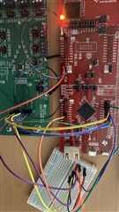
Thanks
Ram.