DAC39J82EVM: Connections with the FPGA and clocks

Part Number: DAC39J82EVM
Other Parts Discussed in Thread: LMK04828

Tool/software:

Greetings,

I am trying to use the DAC39J82EVM with a ZCU102 board and I am having quite a bit of difficulties to set it up. In particular, I requested and received the TI-JESD IP that comes with a reference design for the ZCU102, which is what I'm trying to implement. The reference top design has 4 clock signals that need connection, and the constraints file that comes with the reference design has the following pins assigned:

Clock signal Pin name FMC Pin DAC3XJ8XEVM schematic
sys_clk_p CLK1_M2C_P G2 Not assigned
refclk_p GBTCLK0_M2C_C_P D4 GTX_CLKP
sysref_p LA22_P G24 Not assigned
tx_sync_n LA26_P D26 Not assigned

Now, if I understood corectly how these clocks work:

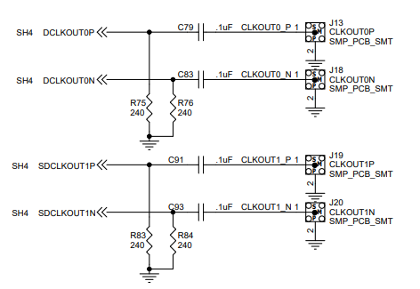
  • sys_clk_p should be routed to a clock with frequency LineRate/80 (for my data_width=64). I assume that, on the DAC schematic it should be connected to FMC_DACCLK_P, so FMC pin D8. Once I know the linerate I understand I need to modify the clocking wizard present in the reference design to match the frequency of this clock and the wanted generated clocks.
  • refclk_p I think is routed correctly to GTX_CLKP
  • sysref_p I understand should be conected to FMC_SYSREF_P, which corresponds to FMC pin D11

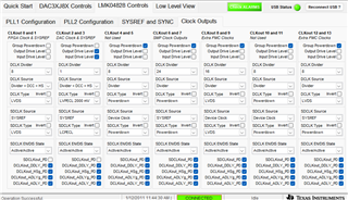
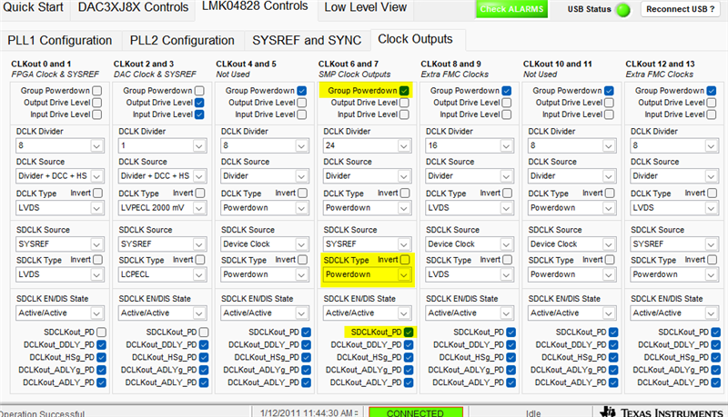
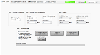
With this in mind I set the GUI with the following parameters

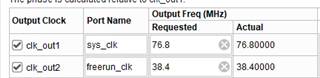
Which would mean that the sys_clk clock should have a frequnecy of 38.4 MHz, so I set that as the input frequency in the clocking wizard. Moreover, when I set the parameters in the Transceiver Wizard the minimum frequency I can set is 76.8 MHz instead of 38.4 MHz for the Actual Reference Clock, which I assume corresponds to the sys_clk generated with the clocking wizard from the sys_clk_p(n) pair coming from the DAC board.

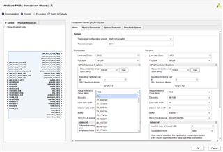
On the other hand, on the Physical Resources tab, the free-running clock frequency is set as a mximum of 38.4 MHz, and I assume this should match the frequency set to the freerun_clk output of the clocking wizard. With these two values, I set sys_clk frequency to 76.8 and freerun_clk to 38.4 in the Clocking Wizard.

I added 2 debug signals for sys_clk and sysref to be taken out some PMOD in the ZCU102, and with the configuration I mentioned I see only noise. If I try modifying the pins to what I assumed are the correct ones, Vivado throws me an error [Place 30-681] for sub-optimal placement of the clock-capable pin and MMCM pair. Any idea on this?

Thanks,

Matías.

  • Matias,

    If the serdes rate is 3072Mbps, then serdes/80 will be 38.4MHz. This is the sys clock frequency required if using data width of 64. The transceiver reference clock can be anything that is a legal frequency for the transceiver. In this case, it looks like serdes/80 is out of the acceptable range for the transceivers, so vivado is forcing the reference clock as twice this, so 76.8MHz. This is a normal occurence when the serdes rate is on the lower end. The freerun clock in the Physical Resources tab of the transceiver wizard will be set as 38.4MHz. Can you confirm the transceiver reference clock divider is half that of the sys_clock to achieve a serdes/40 for the refclk? Can you share the full error?

    Thanks, Chase

  • Hi Chase,

    I can confirm that sys_clk frequency is twice the one for freerun_clk that I assume is the one going to the free-running clock of the Transceiver Wizard.

    Now after trying to re-compile, I don't get the sub-optimal placement anymore, which is weird. Moreover, before I tried also to change the Clocking Wizard primitive to PLL instead of MMCM to avoid the error I mentioned, and from the ports on the PMOD of the ZCU102 I see no signal from them on the scope, and a weird random signal coming from sysref (which also appears even with the EVM board disconnected, so it seems even weirder). Also, from the DAC3XJ8X GUI I see an alarm for DAC PLL Out of Lock

    Could that be an issue? I have the EVM clocking mode to Onboard so it shouldn't depend on the FPGA.

    One other thing I saw with the scope were the signals coming from J21 pins 1 and 3 (SYNC_N signals). One of them seems to be always on, the other one always off.

    Are the schematics of DAC3X8JXEVM correct? Because I can't seem to get clocks from any of the ports. I am part of a research group and we have some projects currently stalled because I can't get this system to work.

    Thanks!

  • Hi Matías,

    Can you export and share the gui config file? What revision of the DAC EVM do you have?

    I haven’t ever taken out signal over the PMOD on the ZCU102. I have way more history with the DAC itself than with fpga so I can’t offer any insight on why the error is no longer present either. If in onboard clocking mode, the LMK typically provides a direct clock to the DAC based on a clock output group. If you aren’t using the on chip PLL for the DAC then this can be ignored.

    Thanks, Chase

  • Hi again,

    Timezone differences make it a little hard to keep the conversation going haha. I have revision D of the DAC EVM. Here I attach the config file for the board. One more thing I tried is checking the SMA ports on the board itself (J1, J3, J5, J7) to see if they were outputting clock signal and I see nothing.

    I also added a "pll_locked" signal to be seen on the LED of the ZCU102, and it's never on, meaning that the PLL receiving the sys_clk is not locking. My hypothesis right now is that the clock is not being sent.

    DAC3982_config.cfg

    Thanks again,

    Matías.

  • Hi Matías,

    I just checked this config and it looks like the LMK settings are very off for onboard clocking. I just tested this mode and it works, albiet the dividers are not set for your case. My config is attached. 2457p6M_821_hsdcpro.cfg

    The reason why is you will not be able to achieve an output of 38.4MHz using this clock divider in onboard clock mode. This LMK04828 has a max output divider value of 32, and currently the VCO frequency is 2457.6MHz, so the lowest output frequency possible is 76.8MHz.

    To achieve serdes/80, you will have to modify the board by removing R16, R18 and adding C12, C16. This will let you drive the DAC with 2457.6MHz signal and then provide a lower frequency reference to the LMK04828. Providing a 1228.8MHz reference to LMK will work and let you set divider as 32 to achieve 38.4MHz. For more headroom, you can use a 614.4MHz reference and use divider of 8/16 to achieve 78.6MHz/38.4MHz respectively.

    Alternatively, if you change to 32 bit RX data width then you can use serdes/40 with onboard clocking.

    Thanks, Chase  

  • Hi Chase,

    I see. I will change my DAC input rate to 1228.8 MSPS, to have LineRate at 6144 Mbps. This configuration should give me a clock of 76.8 MHz right? After changing both PLL and Transceiver Wizard I can set both refclk and freerun clk frequencies to 76.8 MHz.

    I re-compiled the FPGA code to be compliant with these changes, and I still don't see signal coming from both the probe on the PMOD and the DAC (even with your configuration file). I tried changing the constraints to both what they gave me in the reference design and the ones I think are correct. When trying the ones I think, I see something that resembles a clock signal as an output of tx_usrclk_2 from the Transceiver Wizard, but with random frequency and pulse width (each single trigger I do looks like a clock, but from one trigger to the next the shape of the clock changes).

    Could it be that both the Schematic AND the constraints they gave me in the reference design are wrong?

    Regards,

    Matías.

  • Hi Matías,

    Is the PLL2_LOCKED led (D7) lit? Do you see any activity from the extra LMK output SMP ports now?

    The schematics on the web for this board are correct, I just checked myself. The constraints for the ZCU102 will also be correct. We would have caught some mistake with them. I think your issues are still LMK related.

    Thanks, Chase

  • Indeed, the PLL2_LOCKED led is lit, but from all SMP ports I see nothing.

    With the constraints you mean that the one they provided in the reference design should be the correct ones, or the ones present in the schematic? Because the ones coming from the reference design do not match the schematic ones.

  • Can you share a picture of the Clock Outputs tab with all the dividers? The schematic is correct. The constraints are also correct for Vita specifications, but I think this DAC EVM is not in compliance with that so use the schematic of the DAC EVM and the ZCU102 board as reference for defining the FPGA ball connections.

  • Sure, this is a picture of the Clock Outputs tab when setting Quick Start with the following parameters

    Meanwhile, this is the Clock Output tab when using your cfg file

    In both cases, the PLL2_LOCKED led is lit.

  • Can you change the DCLK Type from powerdown to LVDS for the CLKout 6/7 group and then see if you see an output on the SMP connectors?

  • Just did, still nothing out of the SMP connectors. Also unticked Group Powerdown to check if it changed something, but still nothing.

  • Does the board need to be connected to the FMC to check the clocks through the SMP ports? If not I can test other 2 DAC EVM boards we have to see if they all behave the same way.

  • The board does not have to be connected to the fpga card for the LMK to function. Please check on your other boards. Until you can see the SMP port output for the spare LMK outputs then I don’t think there’s much to debug. That’s kind of a road block at the moment. This is a perfect example of why we add those spare outputs to begin with so we can make sure the LMK is behaving like we suspect. 

  • Hi Chase,

    We just tested all 3 of our EVM boards, all with Quick Start config and your config file, while also setting all DCLK and SDCLK types and ticking and unticking Group Powerdown on all clock outputs (basically checking every possible configuration of everything). None of the boards are outputting anything through any SMP ports.

    What is the chance of all 3 boards being faulty? Is this what we are seeing? On all 3 boards we see the PLL2_LOCKED led being lit, so the LMK is at least genereting a clock, just that we can't see it anywhere.

  • Hi Matías,

    I would say there is a <1% chance that all 3 boards are failed.

    Just to confirm, you are measuring at the J13 or J18 SMP connector, right? Not the J1,J3,J5,J7 SMP ports like you mentioned before? Those are for DACCLK and DAC SYSREF input. The J13/J18 outputs are connected to LMK output DCLKout6. The SMP connectors J19/J20 are connected to DCLKout7, which can be used to check that SYSREF is working. Instead of setting to LVDS, please try LVPECL2000mV. From memory I had thought these were LVDS terminated but it turns out these are LVPECL.

    Thanks, Chase

  • You can try to probe at the C79 or C83 pads or the SMP connector positive leg, rather than the actual SMP connector pin. Those are fragile and usually break after 10+ connections. What are you using to measure this also? A spectrum analyzer? Oscilloscope? Is the equipment capable of measuring a signal that is in this frequency range? You can set the divider to its max value (32) to try and lower the frequency so it is easier to capture. 

  • I was, in fact, measuring at the incorrect SMP ports. Now when using the Quick Start interface I see a 153.6 MHz clock being generated from J13 and J18 (when changing the divider to 16 to match CLKOUT0). From both J19 and J20 I still see nothing though. This also happens with your configuration file

    Sorry, that was a stupid mistake from my part, but thanks for pointing it out!

  • Ok, cool! I cannot tell you how much time I have spent looking at the wrong port or debugging something without a clock connected. These are complex devices and its easy to get mixed up.

    The J19/J20 pins won't have any output in the config I sent, the SYSREF output type was set as powerdown. If you change that on the clock outputs tab then these should come up as the SYSREF frequency programmed by the SYSREF tab's divider value. Also, I forgot the main group powerdown was ticked but you had to have noticed that and unticked it, otherwise there would be no output.

  • Ok, after checking some settings around, just changing the configs in the Clock Outputs tab is not enough to see a signal. I can see a 153.6 MHz clock but it's at like 5 mV pk-pk so it's probably cross-talk noise.

    Nonetheless, if I go to the SYSREF and SYNC tab, and set the SYSREF Source to SYSREF Continuous, then I am able to see a not-locked clock with frequency depending on the SYSREF Divider.

  • One more thing, I connected it to the FPGA and still see nothing on the debug ports I created to take out sys_clk and sysref. I tried modifying the divider in the sys_clk but nothing changes. I also tried changing the constraints to the ones provided in the reference design, but also nothing.

  • Strange. I will build and test a reference design from scratch for the ZCU102 and DAC39J82EVM in 821 mode. Hopefully that will help clear things up. I’ll make one like we would usually do which is very basic then also try adding your debug signal to the pmod to see if there are any errors like you saw before.

  • Great, thanks! I tried one more thing. A very simple program that just takes the two clock inputs (sys_clk and sysref) and passes both of them to an IBUFDS primitive (which should just take the differential clock and create a single ended signal), and its output I take out of the PMOD. This way there is no JESDB logic going on, just moving one port to the other. I still see the same weird behavior, that looks like a clock that is not locking properly, even though the output of J13 looks perfect.

    When disconnecting the DAC EVM from the FPGA, using the same program I see even weirder signals coming from it. Not noise level, but instead 1 V signals that look random. With the DAC the randomness looks like a clock that is failing to lock (looks like a stable clock by regions and then changes freq and duty cycle randomly until it turns off), intead without DAC it looks completely random peaks. Could this be a faulty ZCU102? Or maybe the constraints are not really correct?

  • I did one last thing because I'm losing sanity now. I created a program that takes literally every input from the FMC port, and I can choose what I take as an output to the PMOD. Doing that, literally no signal in the output looks like a clock except the ones I had before that have the weird behavior. At least it confirms that the constraints I have seems correct.

  • Hi Matías,

    That does seem odd. Can you take a free run oscillator (I’m sure there is at least one somewhere) from the ZCU102 and buffer it and then send it out on pmod and also that original gpio pin mentioned in the previous post? This fully eliminates fmc from the picture.

    Chase

  • Hi Chase,

    I sent a 125 MHz clock internal to the FPGA and I manage to take it out of the PMOD without issue. I have a lot of cross-talk between the PMODs but that should not be a huge issue to debug.

    Matías

  • I tried one more thing. I took the signals from J13, J18, J19 and J20 and put them into the FPGA through the PMODs. Doing that, I see the PLL locked led lighting up. So it's either the FMC port on our ZCU102 is broken, or on the DAC board. I'll try swapping both to see what changes.

  • If you feel comfortable you can lift the DAC EVM up and probe at the FMC pin, just ensure that it does not slip to any other pins. Which FMC connector on the ZCU are you using?

  • Hi Chase,

    On the ZCU102 we are using HPC1 (the only one that makes the board fit). Haven't tried with a scope, but I did connect the board to a Zedboard (that has an LPC, I know), to probe both the clocks. Still I see nothing, so my hypothesis right now is that, somehow, all 3 DAC boards are malfunctioning...

    Matías.

  • Hi Matías,

    Apologies for delay. I will make a reference design and test this first thing tomorrow. Thanks for being patient

    Thanks, Chase