This thread has been locked.

If you have a related question, please click the "Ask a related question" button in the top right corner. The newly created question will be automatically linked to this question.

ADS8556: Not getting a response from Busy while in Software mode

Part Number: ADS8556

Tool/software:

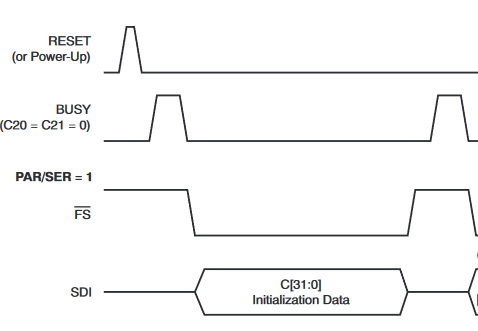
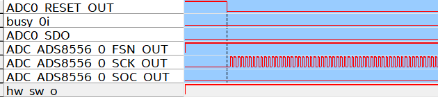
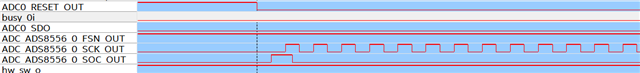
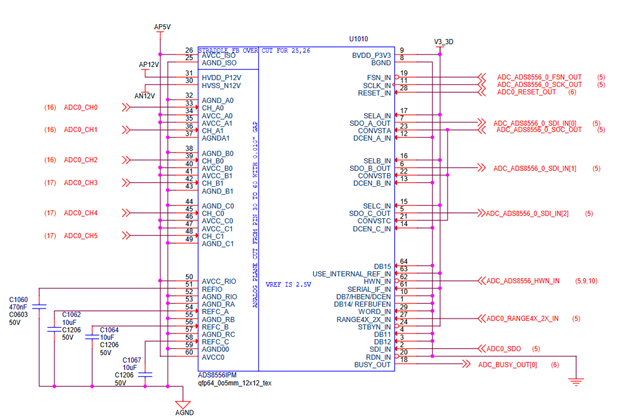
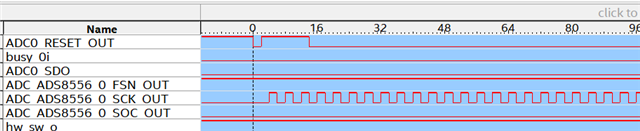
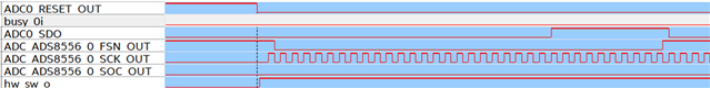
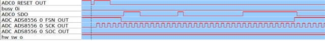
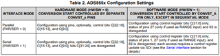
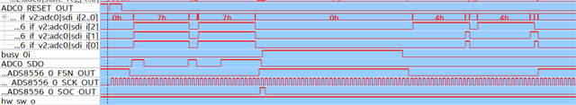
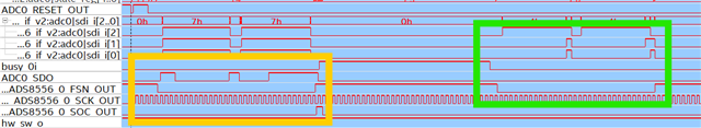
I have a ADC connected into my circuit in serial mode, completely powered up. When hardware mode is active, I get valid responses and communication from ADC. When I drive the HW_SW pin high form software mode, I do not receive the initial pulse on the busy signal from the ADC, nor do I receive a pulse on busy after deasserting and asserting the FS after the 32 clock cycles of SCLK. I'm following the exact sequence shown below but never get a response from busy.

  • Hi Jonathan,

    Thanks for your question! Could you please share an oscilloscope screenshot of your signals including CONVST, CS, BUSY, and RESET? Does issuing a RESET signal fix the issue? BUSY shows that a conversion is in progress. Have you toggled CONVST?

    Best regards,

    Samiha

  • I'm using Signal Tap in Quartus currently as a scope, below are the results from a fresh restart. The SOC signal is a single signal driven to all 3 CONVST inputs.

    I've even tried adding a toggle of the SOC/CONVST signal after the reset, but nothing responds while HW_SW is high.

  • Hi Jonathan,

    Thanks for sharing. Could you try toggling the RESET pin? Reading this E2E thread, it seems sometimes the POR at startup sometimes does not fully reset the device and no BUSY signal is seen, but a RESET pin toggle fixes the issue. Note, the RESET pulse must be at least 50 ns long.

    If this does not fix the issue, what behavior do you see after you set the initialization registers using SDI? Also, are you using the TI EVM for this evaluation or your own board? If using your own board, could you provide the schematic so I can look it over as well?

    Best,

    Samiha

  • I'm not using the EVM board, but I have attached a schematic of how our custom board is setup for the ADC

    I also did a test with a pulse of the ADC reset after the initial POR. I this test, the ADC reset is active for 91.63ns, but still don't see any activity on the reset.


    I have tried sending data to the configuration data across the  SDI without the busy signals, but I'm not sure if they actually are accepted, as busy never responds.

  • Hi Jonathan,

    Looking at your /FS signal, assuming SDI data is being clocked in by the ADC, it looks like CR[31:29] in your screenshot are all zero (by default), so all 3 channel pairs are disabled for next conversion. Could you try setting them to 1 to enable them and see if that makes a difference?

    Your schematic looks good, although it does look like you're missing decoupling capacitors on AVDD. Also, could you try connecting pin 63 to GND, per the datasheet in SW mode in serial mode?

    You could also try setting C17 = 1 to try and see what the CR register contents are.

    What are the SDO (ADC output) contents currently?

    Best regards,

    Samiha

  • Hi Samiha,

    I did try setting CR[31:29] as well as bit CR[21] to try and invoke the BUSY signal, but still no response.

    I talked to my management team about possibly connecting pine 63, but unfortunately we wont be able to do that at this time.
    I will attempt to set CR[17] to 1 to see if we can at least read the register values.

  • Hi Jonathan,

    Understood. C21 should be 0 as we want the BUSY/INT pin to function as BUSY. Also, please note that C16 should be set to 1 to update C[0:23].

    After setting C21=0, C[31:29] = 1, and toggling FS after 32 clock cycles of SCLK, can you try toggling CONVST?

    Also, what is XCLK (pin 27) connected to? This pin should be connected to BVDD or BGND if unused.

    Could you please use n oscilloscope to verify your HVDD, HVSS, AVDD, and BVDD voltages? Also what is the voltage at the ADC inputs?

    Best regards,

    Samiha

  • Hi Samiha,

    I changed C21 to 0, C16 to 1, with C[31:29] as 1. After this is sent during the 32 clock cycles of SCLK, I toggle the CONVST signals. I do get a response on the Busy signal, but I'm not sure what this is in reference to. Does this mean that it accepts the Configuration I sent or something else?

  • Hi Jonathan,

    That is good news! The BUSY signal going high shows that the ADC conversion is in process and that it is responding to the CONVST signal. It is also showing that the configuration was done such that conversion can take place. When the BUSY signal goes low again (after being high), the conversion data is ready to read. You should be able to use the device as needed now.

    Best regards,

    Samiha

  • Hi Samiha,


    We originally would get a Busy signal during normal software mode conversion requests (hw_sw = 0), but it wouldn't go high in hardware mode matching the the documentation in the original post. Since the busy signal responded while being in hardware mode and after making register changes, does this mean that the register changes were accepted?

  • Hi Jonathan,

    I'm not sure I understand the question. The register configurations made in SW mode (HW/SW = 1), with C16 set to 1 so all bits are read, should be written correctly. In SW mode, the device must be configured using the register settings. In HW mode, the external pins configure the device.

    You may set C17 = 1 to see if the control register bits were actually set the way you expect.

    Best regards,

    Samiha

  • Hi Samiha, 

    I have C16 = 1 and C17 = 1, I reran the routine and dropped FSN to 0 after the Busy signal was de-asserted. I checked the values that were returned on all 3 serial data ports (SDI in image below) but the returned data doesn't look correct.

  • Hi Jonathan,

    You'll have to set C[31:29] as 1 too, (and C16, C17 = 1) for the read access. The control registers must be set for every read/write. Let me know if that works.

    Best,

    Samiha

  • Hi Samiha,

    Sorry I didn't mention it in the post above, but yes C[31:29] =1. C[17:16] = 1, and C[9:0] = 1 are sent to the ADC on the ADC0_SDO signal shown in the yellow box. After the 32 SCLK cycles, I assert the FSN and pulse the CONVST signal (SOC_O). In the Green box, once the Busy signal goes low, I drop the FSN to 0 for 32 SCLK cycles to read the registers. What comes back on the serial data lines (sdi_i) does not match what I was expecting. Shouldn't the returned value match the register settings?

  • Hi Jonathan,

    Hm. Looking at your schematic again, it looks like REFIO is grounded, so you would want internal ref to be enabled. Could you set C25 = 1?

    Does the SDO_x data match your expected conversion results? What about when you set C17 = 0? Could you try SDI: C[31:29] =1 in the second frame/access and seeing if that changes the register read data?

    Best,

    Samiha