Tool/software:
Hi everyone,
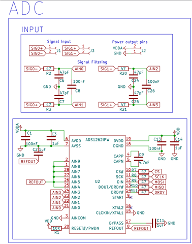
I'm currently working on a circuit design intended to accurately read the values of a load cell while minimizing noise.This values will be read at a max rate of at least 1000sps (or 1200 as I believe that's the closest the ADS1262 can do) I'd really appreciate it if anyone could review the schematic and provide some feedback or suggestions for improvement, as this is my first time working with sensitive ADCs or any analog device for that matter.
Circuit Overview:
- ADC: I'm using an ADS1262 for reading the load cell values. If there are any suggestions for a more appropriate ADC that could further reduce noise or improve accuracy, I'm open to considering alternatives.
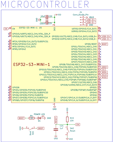
- Microcontroller: The ADC sends its values to an ESP32-S3.
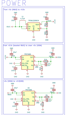
- Power Supply:
- Analog Power: VBUS is boosted to 5.5V, then stepped down to 5V to supply a clean VCCA for the ADC.
- Digital Power: VBUS is also stepped down to 3.3V to power the digital side of the circuit and the microcontroller.
Specific Questions:
-
Power Circuit Placement: I'm debating whether it's better to place the power circuits and the microcontroller on a separate PCB from the ADC to reduce noise and interference. Alternatively, could a good layout with proper separation between the analog and digital sides on a single PCB achieve the same noise reduction?
-
Noise Minimization: Are there any specific components, layout strategies, or filtering techniques that you would recommend to further minimize noise in this type of circuit?
-
Component Suggestions: Is the ADS1262 the best choice for this application, or is there another ADC that would provide better performance in terms of accuracy and noise reduction?
I've attached the schematic for reference. Any feedback, suggestions, or insights would be greatly appreciated!
Thanks in advance!