


Hello
I am using ADS41B49 (14bit ADC but only use D2_D3 ~ D12_D13 as 12bit)
input signal(lvds) is positive so I think I should select offset binary mode
how can I set initial register? I tried to set below map (test pattern is ramp mode)
|
REG_Add |
DESCRIP |
register |
|
|
00 |
RESET |
02 |
|
|
03 |
High PERF |
03 |
|
|
25 |
Gain & TEST_PATTERNS |
C4 |
|
|
3D |
DATA FORMAT |
E0 |
|
|
41 |
LVDS Setting |
40 |
|
|
4A |
HI PERF |
01 |
|
|
BF |
OFFSET |
80 |
the output is
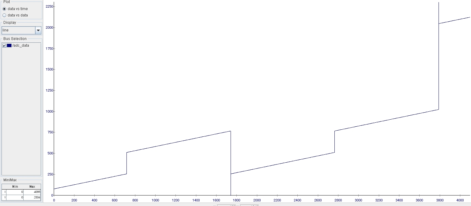
MSB 2bits (D13_D12, D10_D11) is delayed
so I changed the timing (only MSB 2bits) and the output is
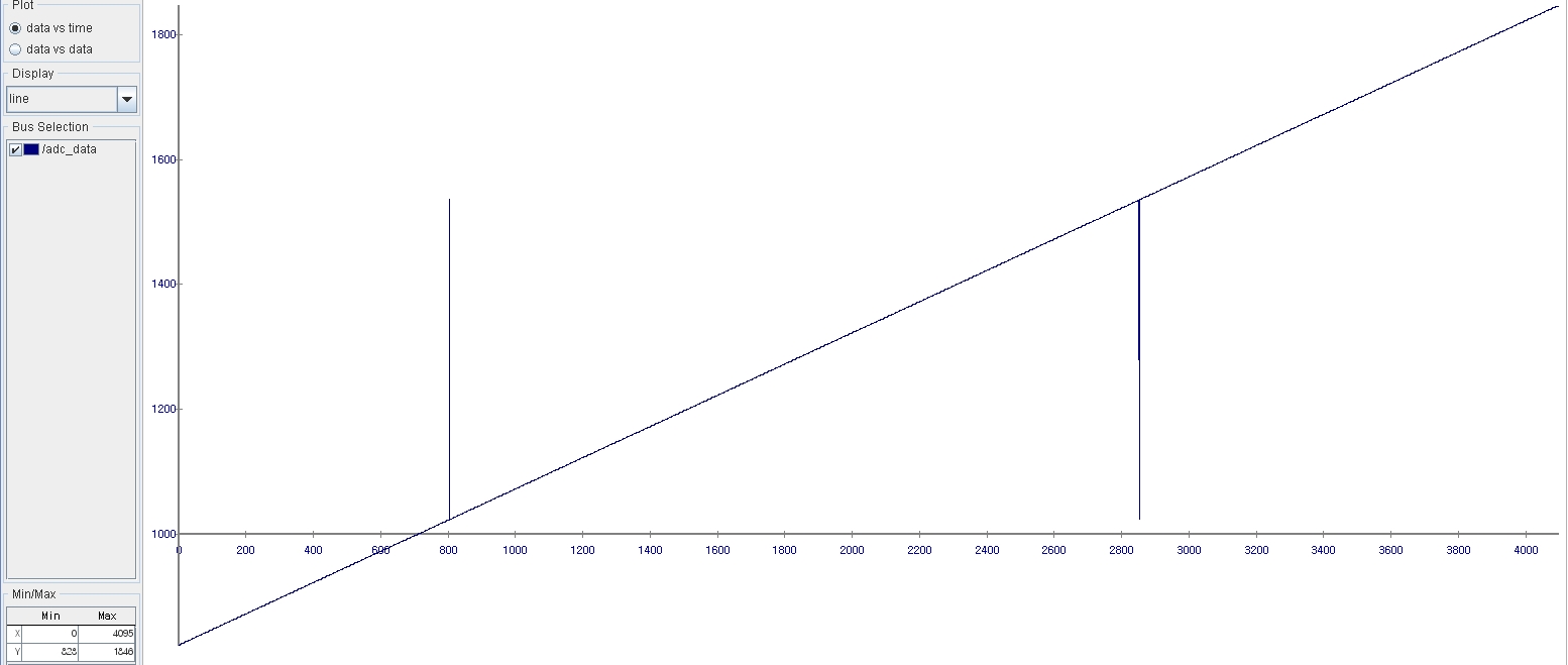
the output is normal
I already checked post (http://e2e.ti.com/support/data_converters/high_speed_data_converters/f/68/t/230210.aspx)
but I don't understand why MSB 2 bits (D13_D12, D10_D11) ?
---------------------------
question is
1. just simple check please about register map
2. I understand D13,D12(Pin 48,47) is toggled as test pattern but D11_D10(Pin 46,45) is also toggled?
3. how can i select offset binary mode to use full scale (0 ~ 4096) ??
thank you
