hi
its since now almost 47th day struggling with ads1256 ic to run this beast but still not able to run this ic
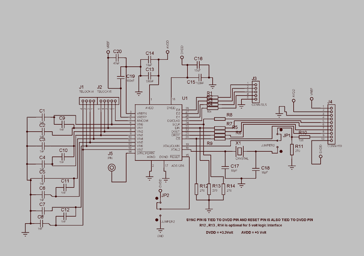
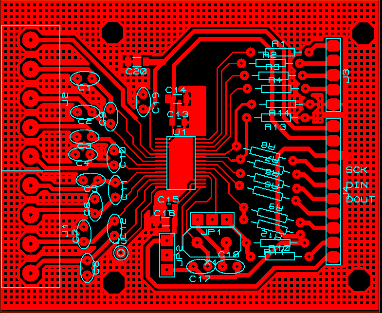
i have constructed prototype pcb to test functionality of ads1256 ic
at first there was no output on serial data out pin of ic at that moment i used 3.3 volt from microcontroller power supply but there was no sine of any data even no signal on ads1256 drdy pin then i had to add dedicated 3.3 volt regulator to ads1256 dvdd power pin then it start showing signal on drdy pin after that since now i am facing strange behaviour of ic
i tried to change output values on digital io pin and it works with out any problem it changes output value i have attached a led to see the result
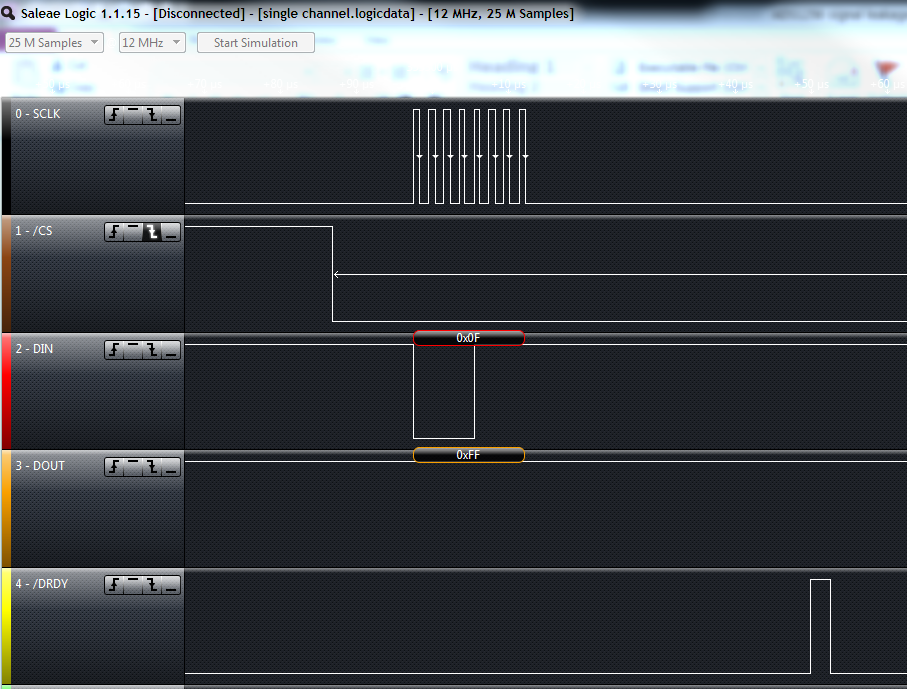
whenever i try to adjust data rate register ads1256 drdy pin shows strange signaling even 1 to 2 second long switching signal on this pin where high and low signal have no correlation that it will be same pattern for all time
then i issue data rate adjust command continuously to set data rate value register it still did not works until i remove power from ads1256 ic and until it starts with default data rate setting and then with multiple issue of data rate adjust command it shows drdy signal as expected
at this point i have these question
why it does not work with common digital power supply rail where many other digital pheripharal work normal and even power supply ripple is less then 20 mv in worse case on its digital power rail
why it requires individual voltage regulator
why it didn't accept command on the first time issue of the command
how many times commands should be issued so it will perform required function specially data rate adjust procedure
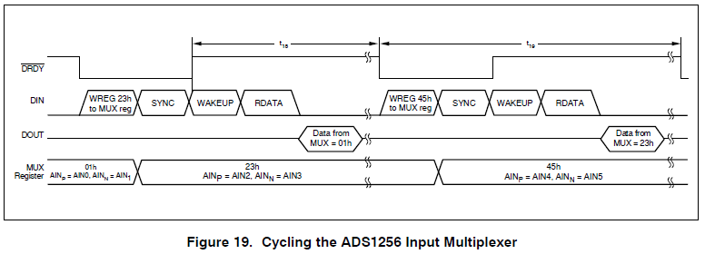
there is no timing digram for data rate adjust command in data sheet and command sequence so what is correct sequence of this command
what is the allowable maximum spi clock frequency @7.2 mhz and @10mhz of crystal oscillator
how to calculate data rate on different clock frequency of adc
we are willing to use this adc in programmable power supply project but this beast is still not functioning properly
hope to get quick reply
regrads
Shams iqbal