This thread has been locked.

If you have a related question, please click the "Ask a related question" button in the top right corner. The newly created question will be automatically linked to this question.

ADS54J66: ADS54J66 won't sync with TSW14J56EVM

Part Number: ADS54J66
Other Parts Discussed in Thread: LMK04828, ,

I've got a custom ADS54J66 circuit - based entirely on the EVM module - that I'm having trouble getting to sync with the TSW14J56EVM.  I'm using the LMK04828 as my clock source, so everything is theoretically set up the same as the EVM.  I've compared all of my clocks and register settings and everything looks good.  However, I can't get the TSW EVM to sync with my board.  Comparing between the ADS54J66EVM and the custom board, the one biggest obvious difference is that I'm not receiving a sync signal from the FPGA when I click the capture button.

D3 is still lit and D4 is not blinking, but I don't know what order things are supposed to happen, so I'm not sure where to start looking.

As an aside, I have a DAC module that has the same LMK part on it and I'm able to sync that to the TSW EVM, so I THINK my clocks are fine (visually, they're almost identical to the ADS54 EVM).

What prompts the TSW EVM to send the sync pulse?  Is there an intermediate step that I should be doing at the register level that will signal the FPGA that I'm "ready to sync"?  I think I've compared all of my signals and registers, so I'm not sure what additional steps to take.

I did change some of my lane assignments... Lane A is connected to FPGA Lane D, for instance.  I thought that would just affect which channels I was seeing in the GUI... would that be a problem with the sync?

Thanks in advance.

  • Justin,

    When the user clicks on capture on the HSDC Pro GUI, this causes the FPGA to send SYNC low and start the CGS process. Once the link is established, the Ref Clock is divided down and sent to LED D4. How many lanes are you using? Your lane swapping may be the issue. Can you send me your schematic and ADC and LMK configuration files so I can take look at them?

    Regards,

    Jim

  • Thanks for the response, Jim. Sorry for the delay.

    I've included both a DAC and ADC schematic in pdf form.  The raw files are in Altium, if you'd prefer them in that format.  The LMK is located on the DAC board, which connects to the FPGA eval board through the samtec FMC connector.  I have a Samtec differential header connecting the DAC board to the ADC board, supplying clocks and passing the digital lines between the ADC and FMC header.

    I'm using 4 lanes and have them matched 1 to 1 with the FPGA... Lane 1 connects to RX0, lane 4 connects to RX3.  I did try updating that in the *.ini file, with no change in results. 

    The board contains 2 ADCs, but I'm only focusing on the one connected to those lanes for this.

    Two excel files are attached showing our register settings.  For this test, I'm loading the LMK with the ADC column.  As noted in the ADC file, I start the SYSREF prior to programming the ADC and shut it off afterwards.  I followed the startup procedure in the ADC user's manual and adjusted any settings to match the EVM ini.

    ADCReg.xlsxLMKReg.xlsx

    ADC.sch.pdfDAC.sch.pdf

  • Justin,

    A block diagram may help me more with this. After looking at the schematics I am assuming your ADC board plugs into your DAC board and the DAC board plugs into the TSW14J56EVM, correct? If this is true, why is there an FMC connector on the ADC board? Is this an option to plug the ADC into the TSW14J56 by itself?

    Can you leave SYSREF running until you get the link configured? What frequency is this running at? What is the ADC sample clock and what is the refclk frequency going to the TSW14J56? When you attempt a capture with the TSW14J56, what message does it report? What is the status of LED's D1-D8?

    I know your LMK is wired differential than the TI EVM but I was surprised there were over 35 register setting that were different. I have not had a chance to look at of this yet though. Did you verify the sample clock and SYSREF at the ADC are present and at the correct voltage levels and frequency? What is the status of the SYNC signal? Does it ever go high, indicating CGS has completed?

    Regards,

    Jim 

  • That is correct, Jim.  The FMC is only on the ADC board for possible use / troubleshooting in the future.  Unfortunately, with the LMK residing on the DAC board, I can't connect directly at this point, so I'm doing everything with the full system.

    I was originally leaving SYSREF running at all times, but tried disabling it, as the EVM board is doing that.  I changed it back so the ADC SYSREF is running continuous, but it didn't appear to help.  For troubleshooting reasons, I'll leave this running, I wasn't sure whether the EVM board shut it down for a specific reason.

    My clock frequencies are as follows:

    ADC clock ~490MHz

    ADC SYSREF ~3.84MHz

    JESD SYSREF ~3.84MHz

    JESD clk ~246MHz

    I've compared the clocks between the EVM board and mine and they appear to be the same frequency for all, given the resolution of my scope.  The ADC sampling clock was slightly lower amplitude than the EVM board (100-200mV lower), but the frequencies were identical when overlaid on the scope.  I tried the 10mA LMK clock at the same frequency, which gave me a slightly different shape, but the same amplitude and frequency as the EVM, but that didn't seem to help, either.

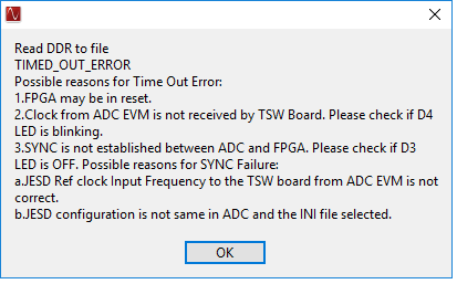
    This is the error I get upon pressing Capture:

    D3 and D8 are lit, none of the others are.

    Almost all of the differences in register settings are due to the additional clocks I'm using.  I've looked through the register map descriptions numerous times, looking at the differences between mine and the EVM, and haven't found anything that should be affecting the ADC/FPGA performance.

    The sync signal is the one that is bothering me.  I never get a state change.  After loading the FPGA and before pressing Capture, the voltage levels are the same between my board and the EVM.  However, with the EVM, there is a state change where there isn't on my board.  I thought this was supposed to initiate the sync between the two, so I'm not sure why I'm not getting it.  The FPGA appears to have SPI communication abilities with the LMK and ADC, so I was worried that it was doing something to the registers. 

    Does the Sync signal change state upon the Capture press?  What are the FPGAs criteria for allowing that state change? 

    I've looked at both SYNCbAB and SYNCbCD signals on my board and neither are moving.  I do see the lines change levels when the FPGA is programmed, so they do seem to be properly connected, but I never see them change state during capture.

  • Justin,

    You may have the wrong frequency for SYSREF. The value this can be is Fs / (K * I) where I is a whole integer. I need to know the exact frequency you are running. The TSW14J56 is using a value of 16 for K when selecting the ADS54J66_4421 option. I am assuming this is the one you are using. If you take 490M and divide it by 3.84M, you do not get a whole integer. Thus the LMK cannot provide the correct frequency. How can you have a SYNC state change on the TSW board but not the ADC board? The SYNC from pins G12/G13 of the TSW14J56 FMC must be connected to the ADC SYNC pins and the ADC configured for only one SYNC mode.

    For every capture click, we reset the Base IP due to which sync will go low and it will go high once the CGS phase is validated by JESD Base IP.

    We reset the Base IP even if SYSREF or REFCLK are the wrong frequency. But if CGS didn’t occur correctly, sync will stay low and there will be no transitions on the signal


    Can you verify the following:

    1.       Is the targeted LMF mode ‘442’ of ADS54J66 with ADC sampling rate as 491.52M

    2.       Is the firmware ‘TSW14J56REVD_RX_ALT_SYNC_LVDS_FIRMWARE’ (FW that Ini file ‘ADS54J66_LMF_4421’ points to) used to get a capture with HSDC Pro

    3.       Can you try with ‘Link Layer Test’ that sends K28.5 (BCBC) characters on data lines and see if there is any change in behavior of the sync signal.

    Regards,

    Jim

  • Good morning, Jim,

    I apologize for the SYNC confusion.  I've got an ADS54J66 EVM board here that I'm using for comparisons with my board.  I see the sync signal change state on THAT EVM board, not the TSW EVM board.  On my custom board, I see the SYNC lines change level when the FPGA is programmed (change from the default 2.2V state), so I believe they are properly connected to FPGA.  Once they initialize, however, I don't see any change in state when I click Capture, which I do see on the ADS EVM board.

    Because I do have the ADS EVM board, I'm currently following the quick start guide completely until I can establish communication.  For this reason, I'm using ADS54J66_LMF_4841 as the ini for the TSW board and setting my ADC data rate to 245.76M, per the guide.  I do want to use 442 in my end design, but using the 4841 gives me a comparison setup.  I believe my clock frequencies are correct (for 4841) because I've been able to compare them with the ADS EVM board using the same settings.  All of the signals between the two boards have been the same with the exception of the SYNC behavior.

    to your questions:

    1. I'm not, but I will try that with an updated SYSREF.

    2. Yes, that is the firmware that is listed in the bottom corner of HSDC Pro

    3.  I'll update that, as well, and look for changes.

    Thanks again for your time, Jim.

  • Hi Jim,

    The layer test didn't help, but I think it did offer some insight into the order of things between the two boards.

    1) Once the FPGA is programmed, it immediately pulls SYNC low
    2) While SYNC is low, the ADC is continuously putting out the K28.5 - I believe I proved this to myself because while in that state, using the Link Layer Test did not change the output, both on my board and the ADS EVM
    3) User hits capture, which prompts the FPGA to look for the K28.5 sequence on the data lines.
    4) Once the sequence is seen, the FPGA asserts the SYNC line high
    5) The ADC then sends lane alignment data followed by sampled signal data
    6) When the FPGA sees this data as valid, it samples the clocks and sets the proper LEDs.

    I repeated these steps with the ADS EVM and when I set the Link Layer Test, the SYNC line did go high, but the LEDs did not change to show a proper sync.

    Does that sound correct?

    With this in mind, it seems I may have an issue with my data lines (which may be an artifact of hanging that spare FMC connector off of them at high speeds).  My next step is to reduce my clock speeds to the point where the data looks the same between my board and the ADS eval board and attempt a sync that way.

    Note:  I am using only the SYNCbAB line and have the registers set accordingly, but I terminated my SYNCbCD lines improperly - both are pulled to GND through resistors.  Would this cause the K28.5 data to be incorrect while SYNC is low?

  • Justin,

    Do you have anyway to get both pairs of SYNC signals to the ADC? For some reason, this is the only way I can get the ADC EVM to link up to the capture board. The part should only need one of these per the data sheet but I cannot get this to work on our setup. I am looking into this and will let you know what I find out. This may be your issue if you are using only one SYNC pair.

    Regards,

    Jim 

  • Justin,

    By default, the part is setup to use both SYNC's. The user needs to change the channel CD to use SYNCAB. This can be done as follows:

    0x4004 0x69

    0x4003 0x00

    0x4005 0x01 

    0x6001 0x01

    0x7001 0x21.

    I tried this on our EVM and it worked with firmware using only SYNCAB.

    Regards,

    Jim

  • Thanks, Jim.  I was programming both 0x6001 and 0x7001 to 0x01, which I thought forced both channels to use SYNCbAB.  I tried to update that, but I came across another interesting issue.

    I've been programming with "LMK_Config_LMF_4421_491p52_MSPS.cfg" and "ADS5xJ6x_2x_N_4_Fs_16_mode_4.cfg" as a baseline,  per your recommendation above.

    I slowed my clocks down 4x (to 122.88MHz by changing the ADC DCLK from 0x66 to 0x78) so i could better capture the data using my 2.5GHz scope.  I manually changed this on the EVM and I was still able to sync, so it seemed like a good place to start where I could monitor all the lines to look for differences.

    Looking at the JESD lines, I was able to see that I was sending data at 2x the intended rate, so I double checked and my JESD PLL was set incorrectly.  While incorporating your changes, I updated my JESD PLL from 40x to 20x (recommended setting for mode 4).  When I made these changes, however, the data being sent to the FPGA changed.  I'm not able to sync, but I can see how that would be an issue if the FPGA is expecting a specific data sequence.  I backed out of all of the changes and isolated just the JESD PLL change and it does appear to change my output.  It does not, however, change the output on the EVM.

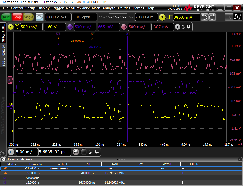
    All of these traces were taken single ended on the same line ( I don't have an RF diff probe available).

    The top trace is my board with the JESD PLL set to 40x.  The second trace is from the EVM board with the proper JESD PLL.  Looking at the markers where I was starting the beginning of each data packet, you can see that the duration of the top trace is have that of the second trace, but the data looks to be the same.  To prove this to myself, I changed the JESD PLL on the eval board to 40x and the two traces overlaid each other perfectly.

    In the third trace, however, I changed only my JESD PLL to 20x and left all other settings the same.  As you can see, the actual data being passed is now different.  I switched back and forth and changing that register caused the data to change.  I tried this with normal operation (SYNC held low), as well as with the link layer test (both 0x40 and 0x60) and the same situation occurred. 

    I feel like I'm REALLY close at this point... any idea what could be causing that data to change?  I thought it was always supposed to send the K28.5 data while SYNC remained low.  I ran this over time, as well, and the same pattern seems to repeat continuously.  Again, it seemed odd primarily because making the same change to the EVM only caused the timing to change, not the data sequence.

  • Justin,

    Is SYNC high or low with these screen shots? If it is high, you should be able to look at the data using signal tap. This ADC has a minimum sample rate of 250MHz. At 122.88MHz, the serdes may not be working properly. Can you double this rate to 245.76MHz and see how the data looks then?

    Regards,

    Jim

  • Hi Jim,

    SYNC is low for all of the waveforms.  I haven't gotten my board to go high yet, so I wanted to make sure the comparison to the EVM was equal.

    I tried changing the clock frequency to 245.76M (register setting 0x6C) while keeping the JESD PLL at the correct setting of 20x.  Unfortunately, the data was still different from the ADS EVM.

    I did finally find a bit of success!  It's using settings that aren't correct, but I was able to sync (not pass data).  By setting the clock frequency to 245.76M and the JESD PLL to 40x on my board, the data was the same as setting the clock frequency to 491.52M and the JESD PLL to 20x on the ADS EVM board.  Using these settings and setting the data rate to 245.76M, I was finally able to establish a sync! 

    Again, I wanted to verify these settings on the ADS EVM board.  However, I noticed that the ADS EVM board had register 6A0016 set to 0x00.  I had been setting it to 0x02 for 40x PLL and 0x01 for 20x PLL.  The data sheet is very confusing on that register (it says JESD PLL should only be 1 bit in the description, 2 bits in the register map).  That could explain why I was getting strange data when using a setting of 0x01.

    I tried changing to 0x00 on that register and the behavior got even more strange.  Before delving into that behavior, should 6A0016 be set to 0x02 for 40x PLL and 0x00 for 20x PLL?

    I'm happy to have at leave achieved a sync, it suggests that the issue is somewhere in my ADC registers.  I'll look for other "gotcha" registers in the mean time and compare directly to the ADS EVM settings using the GUI.

  • Hi Jim,

    I've had a bit more luck today after setting 6A0016 to 0x00.

    With my clocks running at 122.88MHz, I now see the same data on my board as on the ADS EVM board.  It still doesn't sync, but at least I have some SYNC action.  After pressing the Capture button on the GUI, my SYNC line now goes high for approximately 5ms before going low again.  The sync LED (D3) is no longer lit, but D4 has not started blinking.  After this happens, the data on the JESD lines changes, but is still repetitive.  The ADS EVM board looks to be sending real data (I have nothing on the ADC input, so I expect low readings).

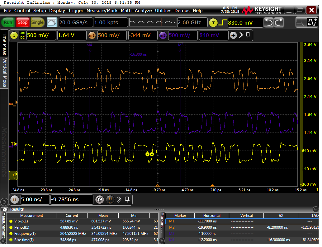
    The top is the JESD data before Capture is pressed.  The second line is the data on my board after the SYNC line pulses (it is low again at this point).  The third line is the data on the ADS EVM after the capture button is pressed. GUI data rate was set to 122.88M in both cases.

    Per your recommendation above regarding the sampling rate, I tried increasing my ADC clock speed to 491.52M (with 6A0016 set to 0x00).  When I do this, the SYNC line immediately pulses high for a short duration - before the Capture button is pressed - and D3 is not lit.  I can hit Reset Board under the instrument options in the GUI and the same thing happens - the SYNC line pulses high for 5ms and repetitive data shows on the data lines again.  I tried turning off the ADC SYSREF pulses, as is done on the ADS EVM, but there was no change.

    0x0074 on the ADC page (0x0F) is programmed to zero, so I don't expect test data to be output on the lines.

    I decided to repeat my earlier "success" and set my ADC clock to 245.76M and the JESD PLL to 40x.  As before, it appears a sync is made - D3 is out and D4 is blinking - but no valid data is passed (nothing is displayed on the GUI).  I'm not sure if that information is helpful to you or not.

    Thanks again for your time working through this with me.

  • Hi Jim,

    To verify my register settings today, I manually looked through each of the registers listed in the ADC register map. There was a difference in a “fine mix” setting, but aside from that, everything lines up.

    Starting with a 122.88MHz clock rate (and output data rate), I again attempted to sync. Again, when the Capture button is pressed, the Sync line goes high for approximately 5ms and then goes low and stays low and I receive the same error message as before. At this point, D8 is lit, all other status LEDs on the TSW EVM are off

    Because my design has lane connections that differ from the ADS EVM board, I updated my configuration ini with the following line:

    Lane Mapping   lane0:0,lane1:1,lane2:2,lane3:3

    It didn’t seem to have any effect when I ran it on the ADS EVM compared to the default, but I kept that as the ini file while using my board. I noticed a LaneSync entry in the Dynamic Configuration menu from the Instrument Options drop down. When I enter 0 or 2 in that location (1 is default), D4 begins blinking when I hit the capture button and I do not get the error message. D4 does not blink if I use 1 or 3 for that variable and I do get the error message

    I repeated this with an ADC clock of 491.76MHz and a data rate of 245.76M. As was the case yesterday, D3 went out before I hit the Capture button. When clicking Capture or resetting the board via the Instrument Options menu, I see the Sync line go high for 1-5ms and then go low again. After the capture button is hit, I get the error message. By selecting 0 or 2 as the LaneSync variable, D4 begins blinking and D3 remains out and I do not get the error message. This appears to be a sync, but there is no data displayed on the GUI (the SYNC line is low here, as well).

    In all cases above, the only register setting I have changed is the ADC DCLK in the LMK. Everything else remained constant.

    I ran a link layer test, as well, and the behavior remained the same. 

    Any thoughts on what to try next?


    Thanks

    Justin

  • Justin,

    Sorry I have not gotten back with you. Have you made any progress with this? Any more information regarding what you tried since your last post?

    Regards,

    Jim

  • Hi Jim,

    I've had some success and a lot of failures... at this point I'm just very confused. I apologize in advance for the essay.

    As I noted in the last post, it seemed I was synced, but there was "no valid data" being passed. After looking into it a bit more, i realized that all zeros were being passed to the FPGA after a sync. I tried many different things, but was never able to get it to pass real data. I triggered on the SYNC pulse and looked at the data being passed (still using the lower speed comms) and I did see the ILA sequence, but even during that mode, the data being passed was always the same pattern - what I think is all zeros.

    In an effort to try out the test patterns, I used the ADS EVM to get the correct settings to connect with mode 8 - according to the data sheet, these patterns only work with mode 8. I was able to sync with the EVM board, but was still having issues syncing with my board. I went back to my register-setting code and noticed that there was a write I wasn't performing... once I write 0x00 to register 0x0F74 (the register that contains the test pattern selection), I was able to sync and pass real data, albeit at a slower speed. However, 0x00 is supposed to be the default for that register, so I didn't think i needed to write to it. After doing this, I was able to select the ramp test pattern and verified it on the GUI.

    With "success" here, i attempted to speed up my data rate, but wasn't able to sync again. I reduced the speed and things worked well, so I tried looking at the bit rate tests under the SERDES test options menu, but that test never actually showed me anything on the screen. I tried on the ADS EVM board and I didn't get any results there, either.

    Given that I had been able to connect at a higher speed using mode 4, but wasn't passing data, I reverted to those register settings to see if I could pass data in that mode... no luck. I again wasn't able to sync (the SYNC line wasn't changing state again). I tried a few different clock settings and data rates and nothing would connect. I decided, for no particular reason, to set both the JESD mode and the K value at the same time by writing a 0xC0 to 690000, followed by setting the mode and K in the next instructions. Prior to this, I had been writing 0x40 t0 690000, set the JESD mode, then write 0x80 to 690000 and set the K value - the method suggested in the datasheet for bring up. I was then able to connect to the board at the lower speed, but not the higher speeds.

    It seems rather confusing, so I guess I have a few high level questions about register programming.

    1) On the LMK and DAC, I program all of the registers. On the ADC, I'm only programming the registers that are changing - this was largely due to the fact that I was following the datasheets on recommended start-up sequence. Should I be writing ALL of the registers, regardless of whether that is just writing the default value?

    2) Similar to what is above. but do you happen to have the register programming sequence that is used by the EVM? Having the behavior change when I programmed the JESD mode and K value separately and together was a bit unsettling... I feel like there may be other similar settings that may be tripping me up.

    3) Is there anywhere I can find the recommended JESD clock vs ADC clock settings?  Would these change with JESD PLL settings in the ADC?

    I've been able to change communication rates using the ADS EVM board WITHOUT changing the JESD clock, even though the HSDC GUI says it should change. That may be causing issues when I try different communication rates - so far, I've only used 122.88M, 245.76M, and 491.52M.

    4) Depending on my settings, sometimes I have to choose either "0" or "2" for the LaneSync option in the Dynamic Configuration menu. What does this option do and might this point to a flaw in my layout?

    5) is there a trick to getting the SERDES test to work properly? The test progress bar runs for 10 seconds or so, then stops and nothing shows up on the screen.

    I'm going to go back to mode 4 and see if I can't get back to where I was a few days ago. Thanks again.

    justin

  • Update:

    I slowed my clocks in mode 4 and synced without issue today. I then sped the clock up and am communicating at 245.76M. This is good news, except for the fact that I didn't actually change anything from yesterday when I couldn't communicate. The questions I asked above are still valid. I feel as if there's just some little quirk that I'm not quite understanding.

    I still have the strange behavior at the higher speed, though... I don't have to hit capture for the boards to establish a valid sync. Data doesn't show up on the GUI until Capture is pressed, but D3 is out and D4 is blinking steadily.
  • Justin,

    Some answers added below. I am currently having issues with mode 4 with my setup where I can only get a capture every second time I click on capture. This is something I am looking into. For now, can you try using mode 0? I have attached the two config files I am using. The ADC config file is setup to only use SYNCab.


     1) On the LMK and DAC, I program all of the registers. On the ADC, I'm only programming the registers that are changing - this was largely due to the fact that I was following the datasheets on recommended start-up sequence. Should I be writing ALL of the registers, regardless of whether that is just writing the default value? If you issue a hard reset,  you should not have to write to all ADC registers. We do not do this with our config files.

    2) Similar to what is above. but do you happen to have the register programming sequence that is used by the EVM? Having the behavior change when I programmed the JESD mode and K value separately and together was a bit unsettling... I feel like there may be other similar settings that may be tripping me up.

    3) Is there anywhere I can find the recommended JESD clock vs ADC clock settings?  Would these change with JESD PLL settings in the ADC? What is the JESD clock you are talking about? The refclk going to the FPGA?

    I've been able to change communication rates using the ADS EVM board WITHOUT changing the JESD clock, even though the HSDC GUI says it should change. That may be causing issues when I try different communication rates - so far, I've only used 122.88M, 245.76M, and 491.52M.

    4) Depending on my settings, sometimes I have to choose either "0" or "2" for the LaneSync option in the Dynamic Configuration menu. What does this option do and might this point to a flaw in my layout? I suggest you do not use this setting. If needed, make changes to the ini files used by the GUI.

    5) is there a trick to getting the SERDES test to work properly? The test progress bar runs for 10 seconds or so, then stops and nothing shows up on the screen. I have never tried this but I think this just sends data across the link. There is no CGS, or ILA information so the link will not get established.

    Regards,

    Jim

    ADS5xJ6x_2x_Fs_4_mode_0_sync_ab.cfgLMK_Config_LMF_4841_491p52_MSPS.cfg

  • I found the cause of the strange sync behavior.  I didn't realize that all 8 lanes are routed through the FPGA and my second ADC is causing the premature sync.  When I shut that ADC down using the global power down, the FPGA EVM behaves properly.

    As an aside, by adjusting my lane mapping, I can read all 8 channels using the GUI, so that was a nice surprise.

    FYI

  • Thanks for the response, Jim.

    1) If you issue a hard reset,  you should not have to write to all ADC registers. We do not do this with our config files.

    That was my understanding, which was why I was concerned with the behavior.  On power up, I'm holding the ADC in reset until my clocks are programmed and then, because I was having issues I couldn't track, I do the software resets suggested in the power up sequence.  I'll continue doing that, thanks.

    3) What is the JESD clock you are talking about? The refclk going to the FPGA?

    Yes, that is correct.  When you enter a data rate in the HSDC GUI, you get a pop up that tells you what clock rate to use for the JESD refclk, but that suggestion appears to be wrong.  As I've been attempting to speed my comms up to see where it stopped syncing, I assumed I needed to change the FPGA refclk, but I'm not sure what to change it to. 

    4)  I suggest you do not use this setting. If needed, make changes to the ini files used by the GUI.

    When I find a setting that does work, I have been changing the ini.  I'm not sure what this variable does, though.  Does it change which lane is used for the initial sync?

    5)  I have never tried this but I think this just sends data across the link. There is no CGS, or ILA information so the link will not get established.

    According to the HSDC user's manual (SLWU087d), a sync must be established first and FFT data needs to be displayed.  At that point, I SHOULD be able to use the eyeQ scan to determine the quality of my signals for each lane.  As I'm increasing communication speeds, I'd like to be able to use that feature, but I haven't been able to get anything to display on the screen.  I've tried using my board and the ADS EVM and nothing has come up.  Can you please try that on your setup and see if it works?


    I'll load up mode 0 so we're on the same page.  I think my final design will require mode 5, so I need to ensure I can pass data at 10GBPS.  I'll update shortly.


    Justin

  • Justin,

    The external reset should happen after clocks are provided. There is also a power up sequence that needs to be followed. Are you doing this (see attached)?  

    HSDC Pro calculates the FPGA clock based on the device selected and the sample rate. If you think this is calculating it wrong, can you send me the details of this case so we can double check this?

    I will try the Eye scan test and let you know what I find.

    Regards,

    Jim

    Power sequence.pptx

  • Hi Jim,

    I'm holding the ADC in reset until the clocks are active. I enable the sysref and then release the ADC from reset. Should I pulse reset after I enable sysref, rather than holding the part in reset?

    Unfortunately, I'm not following the power up sequence. According to the datasheet (section 8.1.1 Start Up Sequence), there is no power up sequencing required.
    "Supply all supply voltages. There is no required
    power supply sequence for the 1.15-V supply,
    1.9-V supply, and 3-V supply, and they can be
    supplied in any order."

    In section 9 of the datasheet (Power Supply Recommendations), there's no mention of the 1.15V supply, but the same is said, that no sequencing is required.

    I'll mod my board to give myself the abiliity to do that before proceeding, though.

    Thanks
  • Justin,

    The power sequence thing is new and will be in the next revision of the data sheet. I have never tried holding the reset low like you mentioned. I will check with design team regarding this.

    Regards,

    Jim  

  • Justin,

    Address  6A0016 is also wrong in the current data sheet. It should read as follows:

    Bit 1-7 not used

    Bit 0 = JESD PLL MODE R/W 0h This bit selects the JESD PLL multiplication factor.

    0 = 20x mode

    1 = 40x mode

    I am not sure if you had this set correctly or not.

    Regards,

    Jim

  • Hi Jim,

    I believe Bit 1 is JESD PLL MODE. writing 0x02 or 0x00 to that register doubles the output rate while keeping the same data. Writing 0x01 to that register keeps the data rate the same as 0x00, but changes the output data and will no longer sync - I verified this on the EVM board. I have a screen shot at the bottom of page 1 that shows what I'm talking about.

    Thanks,

    Justin
  • Hi Jim,

    I modified my board to allow me to bring 1.9V up after 1.5V and changed my register settings to the 4841 mode 0. As before, I was unable to sync and there was no activity on the SYNC line. Just to be sure I didn't break something in my rework, I reloaded my 4421 mode 4 code and it synced both at higher clock speeds (491.52M) and lower (122.88M).

    To make sure I was back "even" with the ADS EVM, I slowed the ADC clock to 122.88MHz and left the refclk at 491.52MHz on both my board and the ADS EVM. I looked again at the data being passed to the FPGA and the two were identical - I was able to overlay them on the scope. Using a setting of 61.44MHz on the HDSC GUI, I as able to successfully sync on the EVM board (I was able to sync using a setting of 122.88MHz on the EVM board with the same clocks, btw).

    Because I had that strange behavior on mode 4 where the second ADC on my board was forcing a sync with the FPGA, I put that ADC into global power down and put the primary into link layer test mode 0x60. Same results - data that matched was the ADS EVM was putting out, but no movement on the SYNC line.

    Just for giggles, I tried loading the JESD MODE with 0x00, 0x01, and 0x02 - the config files doesn't mention changing this register and 0x00 is default; The ADS EVM board has 0x01 in that location, which should be 20x mode; The datasheet says it should be 40x mode, which is 0x02. I didn't see any change in both by board and the ADS EVM board.

    Is there any possibility that my second ADC, which is mapped to RX4-RX7, would be adversely affecting the sync in this mode? I have it in powerdown right now, but the lines are still at a DC offset. Would I be better off removing the series capacitors to completely remove that from the FPGA?

    Thanks,

    Justin
  • Justin,

    If you have the FPGA programmed to only look at the 1 ADC, it should be ignoring everything else. I do not think taking off the caps will do anything for you. With just the one ADC board running, are you using SYNCab and SYNCcd for this ADC or just one SYNC?

    I have another possible issue with another register setting. What value are using for page 0x6900 add 0x0? When I run mode 8, if this is set to 0xC0, SYNC never goes high. When set to 0x80 everything works fine. I am checking with the design team to see if the description of bit 6 is wrong. This may be why when you changed JESD modes, you saw no change.

    Regards,

    Jim


  • I have SYNCbAB going to ADC1 and SYNCbCD going to ADC2 (both connected to SYNCbAB at the ADC so they are programmed the same).

    I was currently setting to 0xC0 at 690000h, which is what was used for the 4421 mode 4.  I thought I had been using that when I programmed mode 8, as well.  I changed to 0x80 and it synced!  Going to try increasing my speed now, I would still like to see the eyeQ scan

  • TSW14J56revD_altsync_lvds.zipJustin,

    I was informed by our firmware design team that the ADS54J66EVM required a special firmware drop to be used by the TSW FPGA which had two sets of SYNC outputs. They informed me that this special drop never had Eyescan support. They just built a new version that does and it is attached. With HSDC Pro open, click on the Instrument Options tab then select "Download Firmware" I new window will open that will allow you to navigate to this file. Give this a try. The Eyescan tool will allow you look at all 8 lanes even if you are only using 4.

    Regards,

    Jim


  • Awesome, Jim.  That worked great.  I'm connected, reading all 8 channels, and found an issue with my layout due to the EyeQ scan.

    Can the EQ values from the EyeQ scan be changed in one of the ini files?  I'd like to increase the AC gain on the one bad channel I have and see if my noise floor goes down, but I'm not seeing that variable available.

  • Justin,

    See if this document helps.

    Regards,

    Jim

    4331.TSW14J56revD SERDES Test Options.docx

  • Sorry, Jim, I wasn't clear on what I was asking. I'd like to apply the AC gain to the signal during normal operation - either to one channel or to all channels. It helped immensely for the EyeQ scan, but I'd like to see if that clears up my noise issue or if I have another design issue lurking. Applying the gain during EyeQ seemed to only be applied during the test and didn't affect the data transfer during a "capture". Is that possible in an ini file, or would I need to rebuild the binary?
  • Justin,

    I think I understand your request. Unfortunately, there is currently no way to add this gain using the ini file. The firmware must be recompiled. There is one option you can try. If you set the ADC to use only SYNCab for both channels, you can use the firmware file called "TSW14J56REVD_AEQ_FIRMWARE.rbf that implements adaptive equalization and see if this helps. Our firmware team is looking into what it might take to add AC gain. Can you tell me what settings you changed to optimize the eye? This may be need for the firmware rebuild.

    There is also an output swing adjustment on the ADC. In page 6A00 address 0x1B, there are settings you can change to increase the output swing. Have you tried this?

    Regards,

    Jim 

  • Thanks, Jim. The AEQ firmware, as well as writing different values to 6A001B had minimal effect on my noise floor or the EyeQ scan. They both opened the eye a bit, but it's still pretty ugly. I only tried the min and max values in 6A001B, so I'll probably try a few more to see what changes I see.

    I got good results from the scan when I used a DC gain of 0 and an AC gain of 4. Higher values were better on the AC, but that was enough to fit the eye around the mask.

    Thanks again,

    Justin