This thread has been locked.

If you have a related question, please click the "Ask a related question" button in the top right corner. The newly created question will be automatically linked to this question.

DS90UH948-Q1: DS90UH948-Q1 can't link 947 after system first power up

Part Number: DS90UH948-Q1

Hello Casey,

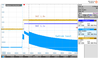
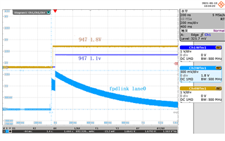
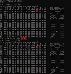
Xiaopeng reported the black screen issue, I located the issue is related with 0x28 register value. The value showed the device don’t go to normal mode(0x19) and keeping in forward channel disable mode(0x20) after the system power up, fail rate 1/15000, and the issue repeatability rate is 100% in the special system(specific 947 and 948).

 Can you help to support on this issue?


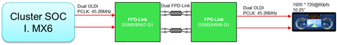
System block as below:


I have confirmed debug result as below:

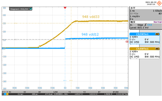
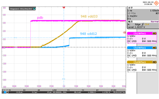
  1. System power sequence(947 and 948) is correct.
  2. The issue can’t be eliminated when turning off/on 947 and maintaining 948 power supply.
  3. STP cable maintaining connecting, the issue can be eliminated when turning off/on 948 and maintaining 947 power supply.
  4. The issue can’t be eliminated When disconnecting/reconnecting the STP cable and turning off/on the 948 power supply at the same time and maintaining the 947 power supply.
  5. When maintaining system power supply, and pull low/high 948 PDB, the issue can be eliminated.
  6. When maintaining system power supply and reset 948 by 0x01[0] bit, the issue can’t be eliminated.
  7. When maintaining system power supply and reset 948 by 0x01[1] bit twice times(once time, issue can’t can be eliminated), the issue can be eliminated.
  8. I have tried to write the correct value into 948 0x28 register manually, but this register can’t be operated.
  9. The 948 register map in attachment.
  • Hello Xiaowei,

    Did you make sure the power-up sequence on bothe sides (i.e. 947 and 948) is as per d/s? Including the timings?

    Did you apply the erratas?

    Are you using any GPIO to control your display? e.g. to control back light of the display?

    Are you using single link or dual link mode?

    Is single or dual link mode detected automatically of forced? 

  • 1,The power-up sequence of 948 does not meet the requirements of the datasheet.

    And we fixed that power-up sequence, but it didn't work, confirmed by Xiaowei.

    2,We have apply the erratas,

    but the question is 947Registers 0xC=0x4,That means no cable was detected, so errata has not been executed at that time

    3,NO,we have not use any GPIO.

    4&5,We used  dual link mode,automatically


    In addition, we found that the FPDLINK waveform of LANE0 and LANE1 was different when the failure(947Registers 0xC=0x4) occurred.

    Please see the picture

  • Hello,

    Yes, if reg 0x0C=0x04 means Link was not detected!

    Can you make sure the Back channel is enabled on the 948? this is in reg 0x01[2]. This bit must be always 1.

    Can you provide reg dumps from 947 and 948 in a good working case, and another reg dumps from failure mode? 

  • Hello, Hamzeh

              Please see the attachment ,Thanks!

           948 & 947 Register compare.xls

  • Hello,

    All the 947 registers are indicating NO Detected DES. Please make sure the DES is powered-up after the SER is up and transmitting forward channel signal, otherwise you need to apply a reset on the DES after receiving the valid signal.

    Also on the Not-working mode, you are forcing the Link in reg 0x5B[0] where in a working mode this is not forced.

    Additionally, in the not working mode, you are writing some reserved bits and registers, such as 0x23 and 0x24 on the 947. Writing those two registers is a part of the errata, but you should write those registers again to 0x00 to make it working proberly. So I believe you are not excuting the errata correctly!!

  • Hello,Hamzeh   

             1,Is there a recommended power-up sequence diagram for 947+948 system?

             2,if Reg0x24≠1B,we're going to keep repeating this step1&2,

              In this case, because 0x24≠0x1b. So the value of 0x24 is constantly changing.That's why 0x24 is not equal to 0x00.

                Step 1:

    • Reg0x23 = 0x80 //Enable read for the power-up state machine
    • Reg0x24 = 0x80 //Enable register-read capability of state-machine in register 0x24
    • if Read Reg0x24[4:0] //Read register 0x24[4:0] for power-up state-machine status

                 //If Reg0x24[4:0] has a value of 5'b11011, go to Step 2

                 //if Reg0x24[4:0] has any other value, re-read Reg0x24[4:0] after a minimum delay of 10ms

                Step 2: Clear registers

    • Reg0x24 = 0x00 //Clear register 0x24
    • Reg0x23 = 0x00 //Disable read of power-up state machine state
  • Hello,

    1) The requirement is to power-up the DES only after the SER has already starts sending valid video signal. 
    Please refer to 948 datasheet figure 9-1, Table 9-1 and Note (1) bellow the table.

    2) This is correct. But in this case you should not go further and use the system before the power-up state machine status has reached 0x1B and after that set reg 0x23 and 0x24 to 0x00.

    If reg 0x24 even after longer time can't reach the status 0x1B this means you have something wrong on your sequence.

    The conditions for state machine reaching 0x1B are:

    a) link has been detected with the connecting deserializer and
    b) serializer PLLs have locked to the input OLDI clock

  • Hello Hamzeh

    We found that 948 was power-on earlier than 947,

    and the power-on sequence of 948 was inconsistent with the 948 datasheet, but our screen supplier approved the design through Taiwan TI FAE.

    Here, I attach the timing diagram of 948, please help us to judge whether the power-up sequence of 948 is correct.

    Thanks so much!

  • Hello,

    the provided Power-on sequence is wrong. PDB can't be switched to high before VDD33 or VDD12.

    Please refer to figure 9-1 and Table 9-1.

  • Hi  Hamzeh

    We have fixed the power-on squences of 948 PDB and 947+948;after power on, the link can be established normally, that's an improvement.


    However, during the execution of 947 errata, it was found that the operation of soft reset 947, reset FPD PLL and reset OLDI would cause UNLOCK, which could not be re-lock for a long time, more than 2min. The normal system would re-lock within tens of milliseconds.

    So in this failure case, errata introduces a new problem,and what shall we do next?

  • Hello,

    This is not normal behavior! Normally you should have LOCK within short time.

    This is only possible if you have instable Input CLK to the 947. Can you please measure this and make sure it is stable?

    Also you need to make sure the DES is also powered-up within a short time after the serializer, other wise the SER will keep waiting for the DES. 

  • Hi  Hamzeh

    I have measured the input CLK waveform of 947, and it is stable when losing the lock, and 947reg0xC=0x4.
    The following figure shows the test process after we delete errata. The screen can display normally after power on, and link is normal.
    After writing 947reg0x1=0x3, 947reg0xC changes from 0x5 to 0x16.The display screen changed from normal display to black screen, which cannot be recovered for a long time.

    At present, the 948 power-up later than the 947 3 seconds,How long should we set ?

  • Hello,

    Can you please send the register dumps in text form? It looks like there are too many differences!!

    Also when did you make these reg dumps? Is one in good case and one in bad case?

  • Hi  Hamzeh

    please see the excel,and I also uploaded the text.

    These reg dumps are taken after the first power on and soft reset,It's good before soft reset 947, bad after soft reset 947.

    And we made the 948 power-up later than the 947 3 seconds.Whether this time is reasonable,and how long should we set this time ?

    947 Register compare after softReset.xlsx

    947 Register after softRese.txt

  • Hello Hamzeh

    Is the sequence between vdd3v3 and vdd1v2 correct?The waveform looks like VDD1v2 arrived earlier than VDD3V3. Does this make a difference?

  • Hello,

    VDD12 should come later or at the same time, but not earlier than VDD3V3/VDDIO.

    Let me review the reg dumps and comeback to you

  • Hello,

    I have seen from the reg dumps that you are writing reg 0x01 to 0x03. Any reason for that? If you want to digital reset the 947, you should write 0x01 to 0x01, otherwise you are resetting all registers to default and you must reconfigure and apply all Erratas again.

  • Hello 

          “Please make sure the DES is powered-up after the SER is up and transmitting forward channel signal, otherwise you need to apply a reset on the DES after receiving the valid signal." 

    Why should the 948 be powered up after the 947 transmitting forward channel signal?

    We want to know why in principle,we need to explain this to our boss.

    Thank you very much!

  • Hello,

    Please refer to Note (1) after Table 9-1.


    Note that the DS90UH948Q-Q1 should be powered up after a compatible Serializer has started sending valid video data. If this
    condition is not satisfied, then a digital (software) reset or hard reset (toggling PDB pin) is required after receiving the input data. This
    requirement prevents the DS90UH948Q-Q1 from locking to any random or noise signal, ensures DS90UH948Q-Q1 has a deterministic
    startup behavior, specified lock time, and optimal adaptive equalizer setting.

  • Hello

    I want to ask some questions about 947,Thanks!

    1,In single link mode, can port1 (DOUT1) be configured to output fpdlink? If it can be achieved, how to configure it?


    2,In dual link mode, will the forward channel send I2C/GPIOs/I2S signals in two links or a single link? If it is a single link, will it be DOUT0 or DOUT1?

    3,The OpenLDI Clock Frequency we input to the 947 is 45M, can we use the dual link mode?

  • Hello Guozhen,

    1) No, this is not possible. Paired with a single channel Deserializer, the primary channel is always port0.

    2) Minimum oLDI CLK in dual mode is 50MHz, and in single mode is 25MHz.

  • Hello Hamzeh

              So, do we need to use forced single link mode? At present, the software is configured with automatic matching mode, why most of them are in dual link mode when power-on? What I understand is that if OLDI Clock Frequency=45MHz, then single link should be used automatically, right?

    And In dual link mode,Will both two forward channels send I2c data?

  • Hello Guozhen,

    Yes, if you are using auto detect, the device should work in single mode.

    Yes, If using dual link mode, both links will have I2C communication.