This thread has been locked.

If you have a related question, please click the "Ask a related question" button in the top right corner. The newly created question will be automatically linked to this question.

TCAN4550-Q1: Schematic & layout review

Part Number: TCAN4550-Q1
Other Parts Discussed in Thread: TCAN4550

Hi Team,

There is a good new that DIN TCAN4550-Q1

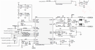
Please help check this SCH & layout, THX

4251.APA-1GBR(06162021).7z1680.APA_20210616.pdf

  • Kygo,

    An applications engineer has been notified of this post and will respond accordingly. Can you share the layout in a different file extension, like .zip or PDF?

    Regards,

    Eric Hackett

  • Hi Kygo,

    I can open your layout gerber files.  I will review these files and provide feedback by tomorrow.

    Regards,

    Jonathan

  • Hi Jonathan & Eric,

    Thank you!

  • Hi Kygo,

    I have reviewed your schematic and have the following comments:

    • VSUP/VIO decoupling looks ok.
    • If WAKE is unused it can be connected directly to GND or VSUP. Using a 0R resistor is ok.
    • If INH is unused it can be left floating. A weak pulldown resistor is only needed when it is used because it is driven high, but becomes Hi-Z otherwise and needs a resistor to pull low.  Having a 100K resistor is ok.
    • RST looks ok. It is an active High signal and there is an weak internal pulldown resistor.  A direct connection to the MCU is ok but will need to be driven Low for normal operation.
    • The SPI pins are a bit confusing between the pin names and net names and there appears to be a possible mismatch that needs to be double checked.
    • The CS pin with net “TCAN4550_CS2” has a test point labeled “CS1” which may not be an error but does not appear to match the “CS2” in the net name.
    • INT has the required pullup resistor and looks ok.
    • GPO2 has the required pullup resistor but a testpoint that says “GP1” which may not be an error, but doesn’t appear to match the pin name of “GPO2”.
    • GND and PAD connections look ok.
    • FLTR pin has the required 0.33uF capacitor and looks OK.
    • VCCOUT pin has the required 10uF capacitor and looks OK.
    • OSC1 and OSC2 pins: The load caps seem to be smaller than what the TCAN4550 will need with most crystals.  
      • I will note that the TCAN4550 will also work with a single-ended clock input which requires the OSC2 pin to be connected to GND.  When using a crystal it is important to optimize the crystal components in the circuit so that the voltage levels of the oscillation waveform on the OSC2 pin do not drop too low and cause the device to think the pin is ground and a single-ended clock is being used.  
      • We also now strongly recommend adding a series damping resistor between the OSC1 pin and the crystal pad that will greatly help optimizing the crystal circuit components for proper operation.  Without a series resistor, the only optimization options are to adjust the capacitor values that may result in a frequency shift or a large drive level.  I recommend adding a 0-ohm resistor that can be replaced with another value later with an optimized value if needed.
    • CANH and CANL pins and components look ok.

    The layout looks ok to me and it appears there will be room for a series resistor between the OSC1 pin and crystal with a little adjustment to the crystal placement.

    Regards,

    Jonathan