This thread has been locked.

If you have a related question, please click the "Ask a related question" button in the top right corner. The newly created question will be automatically linked to this question.

DP83848-EP: Providing Oscillator clock on X1 After power up instead of prior power up

Part Number: DP83848-EP
Other Parts Discussed in Thread: 66AK2G12, SN74AHC541

Hi,
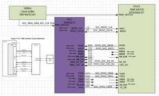
In my new design the PHY DP83848-EP is connected to the FPGA (Xilinx Artix ).
The X1 50Mhz reference clock is provided from the FPGA IO to the PHY to X1 pin 34.
The Datasheet requires clock to be stable for 167mS (table 45.7.1 pag 14 )
I assume the requirement is to have the reference clock toggling before power up and 167mS after power up.
However when sourcing the reference clock from FPGA it takes time the FPGA to have clock out since the FPGA must be configured (87 to 200mS ) all this time the IO floats.
So my suggested solution is to hold the reset of the PHY asserted at power up and during FPGA configuration. Only after the FPGA is up starting to output the reference clock to the PHY, only then the PHY is taken out of reset.
Does this method comply to the request having stable clock prior to power up?

Thanks
Avner

  • Hello Avner

    Thank you for the query.

    The method looks correct. 

    Do you see a way to terminate the floating IO during power up. This is a good to do.

    Please make sure you have the reset asserted for the specified time after the applying a stable clock.

    Please feel free to reach out if you need a schematic review.

    Regards,

    Sreenivasa

  • Thanks Sreenivasa for the fast response.

    Yes during the IO float time the reset can be pulled down and only after configuration completion the  reset will be released.

    Thanks for suggestion for schematic review. The only thing that bothers me is selection of RX_DV or CRS_DV to be connected to the FPGA 

    What is your suggestion if the FPGA is connected to the PHY IN RMII or MII.

    Thanks,

      Avner

  • Hello Avner, 

    Please refer to some of the new devices like DP83822 or DP83826 for information.

    You could consider using CRS_DV.

    Regards,

    Sreenivasa

  • Hi Sreenivasa ,

    Thanks for the Idea to use the newer parts.

    I will consider them in new project. For that one, I will still keep using the DP83848-EP.

    You said that you can review the schematics, so I will appreciate it if you will take a look at the connection diagram between the PHY and the SOC by TI 66ak2g12.

    In this instance of PHY usage the FPGA is not involved. And it is a standard RMII connection to CPU.

    The 50Mhz clock source for both SOC and the PHY is from Oscillator of 50MHZ that is connected to simple buffer SN74AHC541.

    Its skew is not clear but the data sheet states input to output of max 6.5nS.

    Do you think that it is OK with the timing budget (20nsec tis the clock period)


    Thanks

      Avner

  • Hello Avner

    Thank you for the inputs. On a high level the connections look good.

    Please refer to the below document. 

    https://www.ti.com/lit/an/snla076a/snla076a.pdf

    If possible, provide a provision for RX_DV.

    Additional Feature of the DP83848 In addition to RMII defined signals, the DP83848 supplies an RX_DV signal (receive data valid) that allows for a simpler method of recovering receive data without having to separate RX_DV from the CRS_DV indication. This is especially useful for systems that do not require CRS, such as systems that only support full-duplex operation. As described later in this document, RX_DV is also useful for Remote Loopback and Full-Duplex Extender operation.

    For clock buffering, you could use something similar to CDCLVC1102

    Although this is a block diagram and you would take care later, please follow the below 

    TXD[3:2] should be pulled low to put these inputs in a known state.

    Terminating other unused TX signals also is recommended.

    Regards,

    Sreenivasa

  • Hi Sreenivasa,

    Thanks for the tips and fast response.

    Regarding the TX inputs, I have added pull downs to the schematics even though there are internal pull down within the PHY. – Thanks !

    Regarding the buffer – I will change to LMK1C1104PWR which has output to output skew of 50pS max.


    When you say “provide a provision for RX_DV” how you suggest the implementation will be ?

    The SOC have input pin G22  called CRS_DV.

    Do you mean to connect the PHY pin 39 RX_DV instead of pin 40 CRS_DV to the SOC ?

    For the FPGA – PHY connection, (which we write the code), I have connected the RX_DV.

    However for the SOC 66AK2G12ABYT100, I am not sure I can do this.


    Please advise,

      Avner

  • Hello Avner, 

    Thank you for the very well summarized  updates. The design seems be going well and good luck.

    You are right in understanding the RX_DV suggestions.

    If SOC 66AK2G12ABYT100 does not provision for an RX_DV, this should be fine. 

    Regards,

    Sreenivasa