This thread has been locked.

If you have a related question, please click the "Ask a related question" button in the top right corner. The newly created question will be automatically linked to this question.

SN65DSI86-Q1: can't output color bar pattern

Part Number: SN65DSI86-Q1
Other Parts Discussed in Thread: SN65DSI86, TEST2

Hi,

we are using sn65dsi86 to drive panel through DP cable. in order to make sure this can work, we firstly want to use color bar pattern to drive panel. but it didn't work. 

we close ASSR of sn65dsi86, then we configure video related register. lastly, we configure 0x3c as 0x10 to enable color bar pattern. but we didn't see any output on panel.

do you know how to drive the panel with dsi86 internal color bar pattern generator? is there any doc to describe the procedure of enabling color bar pattern to drive panel?

thanks!

  • Hi,

    How did you disable the DSI86 ASSR? To disable DSI86 ASSR, 

    Pull TEST2 pin to 1.8V thru a 1k to 10k resistor. Once TEST2 is high, the following steps must be performed:
    1. Write 0x07 to register 0xFF. This will select Page 7.
    2. Write 0x01 to register 0x16. This will make ASSR_CONTROL to be read/write.
    3. Write 0x00 to register 0xFF. This will select Page 0.
    4. Write 0 to bits 1:0 at register 0x5A. This will change from ASSR to Standard DP.

    Can you share your schematic and panel spec?

    Thanks

    David

  • yes, the step to disable ASSR is the same as what you described. 

  • the panel we used is a Macbook Pro panel, a 15.6' panel.

    the resolution is 2880*1800. the parameter is as below:

    HACT:2880  HBP:80  HPW:32   HFP:80

    VACT:1800  VBP:43  VPW:6     VFP:3

    pixel clock is 337.75MHz

    line clock is 111.102kHz

    we connect sn65dsi86 to a third party driver board through a DP cable. the driver board will drive panel through eDP parallel wire.

    on more question, can i use sn65dsi86 to drive normal PC monitor with DP connector? for example Dell U2419H monitor?

    thanks 

  • Hi,

    The DSI86 can support DP monitor. Looking at the schematic, do you have the 100k pullup on AUXN and 100k pulldown on AUXP?

    Thanks

    David

  • no, we didn't have pullup for AUXN and pulldown for AUXP, is this necessary?

    could you please help to provide a procedure to enable color bar pattern to drive DP monitor?

  • Hi,

    For eDP, the pullup/pulldown on AUXP/N is optional. But for DP monitor, the pullup/pulldown is a must.

    You can use this spreadsheet (script no ASSR) to generate the register value for enabling the color bar, https://e2e.ti.com/support/interface-group/interface/f/interface-forum/945404/faq-sn65dsi86-how-do-i-programming-the-sn65dsi86-registers.

    Thanks

    David

  • Hi,

    as you can see, our DP_PWR is floating. which power rail should we pull up AUXN to?

    for the DP monitor, we don't need to supply DP_PWR, right?

    thanks,

    chaodong 

  • Chaodong

    On the source, the AUXN needs to be pulled up to DP_PWR through the 100k resistor. 

    The DP_PWR on the source side is optional per the DP spec.

    Thanks

    David 

  • Hi David,

    on our board, we didn't supply DP_PWR. the DP_PWR pin was floating. in this case which power rail should we pull up AUXN to?

    thanks and best regards,

    chaodong 

  • Chaodong

    It needs to be pulled up to 3.3V.

    Thanks

    David

  • Hi David,

    if i want to get EDID and information from panel, how can i do that?

    thanks and best regards,

    chaodong 

  • Chaodong

    Please see section 8.4.5.3 I2C-Over-AUX for detailed description, below is example on reading the EDID and the DPCD register.

    This example will read 256 bytes of the EDID.

    <aardvark>
    <configure i2c="1" spi="1" gpio="0" tpower="1" pullups="0" />
    <i2c_bitrate khz="100" />

    ======Enable I2C_ADDR_CLAIM1======
    <i2c_write addr="0x2D" count="1" radix="16">60 A1</i2c_write> />

    ======Write EDID base of 00 ======
    <i2c_write addr="0x50" count="0" radix="16">00</i2c_write> />

    ======Read 256 bytes of EEID======
    <i2c_read addr="0x50" count="256" radix="16">00</i2c_read> />

    </aardvark>

    This example will read 16-bytes from sink’s DPCD registers 0x00000.

    <aardvark>
    <configure i2c="1" spi="1" gpio="0" tpower="1" pullups="0" />
    <i2c_bitrate khz="100" />


    ======Clear Status Registers for AUX Request======
    <i2c_write addr="0x2D" count="1" radix="16">F4 FF</i2c_write> />

    ======Send AUX Request for 16 bytes from DPCD 0x00000 ======
    ===========DPCD Address is 0x00000 ======
    <i2c_write addr="0x2D" count="1" radix="16">74 00 </i2c_write> />
    <i2c_write addr="0x2D" count="1" radix="16">75 00 </i2c_write> />
    <i2c_write addr="0x2D" count="1" radix="16">76 00 </i2c_write> />

    ===========Number of Bytes to Read is 16 ======
    <i2c_write addr="0x2D" count="1" radix="16">77 10 </i2c_write> />

    ===========Send AUX Read Request ======
    <i2c_write addr="0x2D" count="1" radix="16">78 91 </i2c_write> <sleep ms="20" />

    ======Read Status of AUX Request======
    ======Make sure SEND_INT is set and no errors======
    <i2c_write addr="0x2D" count="0" radix="16">F4</i2c_write> />
    <i2c_read addr="0x2D" count="1" radix="16">00</i2c_read> />

    ======Clear Status Registers for AUX Request======
    <i2c_write addr="0x2D" count="1" radix="16">F4 FF</i2c_write> />

    ======Read 16 bytes from AUX_RDATA======
    <i2c_write addr="0x2D" count="0" radix="16">79</i2c_write> />
    <i2c_read addr="0x2D" count="16" radix="16">00</i2c_read> />

    </aardvark>

    Thanks
    David

  • Hi David,

    got it. will have a try later.

    thanks and best regards,

    chaodong 

  • Hi David,

    i can drive monitor with color bar now. but i can't display using data from dsi channel. how can i check whether i have received valid packet from DSI?

  • Hi,

    Can you read the status register 0xF0 to 0xF8?

    Addresses 0xF0 thru 0xF3 report errors associated with the DSI interface. Sometimes errors flags can be set at power-on or during start of the DSI stream. For this reason, it is recommended to clear flags by writing 0xFF and then reading back status flags. The bits which remain set are the errors which should be focused on. Typically errors set in these fields indicate signal integrity issues. Recommend verifying setup/hold meet DSI86 requirements. Also, adjustment of the RX EQ located at register offset 0x11 may help.


    Address 0xF4 report errors associated with AUX communication. AUX communicate typically fails when attempting to communicate with the eDP panel when the panel is not ready. Typically, the panel indicates it is ready when HPD is high. Also, REFCLK frequency not being correct can cause AUX failures.
    Address 0xF5 reports status of HPD. This register is provides status of HPD. This register is only useful if HPD is enabled (register 0x5C bit 0 (HPD_DISABLE) is cleared).


    Address 0xF6 thru 0xF7 report errors associated with DSI to DP video timing. Typically, errors are set in these registers when video timing programmed into DSI86 doesn’t match timing received on the DSI interface. It is important the DSI86’s video registers located from 0x20 thru 0x3A match video timing used by the DSI source. The DSI86 will derive the DP timings from values programmed into these registers.


    Address 0xF8 report errors associated with DisplayPort link training. Signal integrity issue may be a cause of the failures. It may be necessary to reduce eDP data rate and/or reduce the number of DP lanes to correct link training issues. It also may be necessary to change DSI86’s Link Training Look-Up-Table default values. The LT LUT is located from register 0xB0 thru 0xC3. The LT LUT contains transmit voltage swing level and pre-emphasis levels used during the link training process.

    Thanks

    David

  • Hi David,

    0xF5 is 0x02, and 0xF8 is 0x01, all other registers all 0x00.

  • Hi,

    Can you send me the entire DSI86 register programming value?

    Also, if you map the HSYNC/VSYNC to GPIO3 and use a scope to measure the GPIO3 pin, what frequency are you seeing for HSYNC and VSYNC?

    Thanks

    David

  • Hi David,

    plainI2CWriteVal.exe AQT6D0541 0x2c 0xff 0x07
    plainI2CWriteVal.exe AQT6D0541 0x2c 0x16 0x01
    plainI2CWriteVal.exe AQT6D0541 0x2c 0xff 0x00
    plainI2CWriteVal.exe AQT6D0541 0x2c 0x0a 0x06
    plainI2CWriteVal.exe AQT6D0541 0x2c 0x10 0x26
    plainI2CWriteVal.exe AQT6D0541 0x2c 0x12 0x7d
    plainI2CWriteVal.exe AQT6D0541 0x2c 0x13 0x7d
    plainI2CWriteVal.exe AQT6D0541 0x2c 0x94 0x80
    plainI2CWriteVal.exe AQT6D0541 0x2c 0x0d 0x01
    plainI2CWriteVal.exe AQT6D0541 0x2c 0x5a 0x04
    plainI2CWriteVal.exe AQT6D0541 0x2c 0x93 0x34
    plainI2CWriteVal.exe AQT6D0541 0x2c 0x96 0x0a
    plainI2CWriteVal.exe AQT6D0541 0x2c 0x20 0x80
    plainI2CWriteVal.exe AQT6D0541 0x2c 0x21 0x07
    plainI2CWriteVal.exe AQT6D0541 0x2c 0x24 0x38
    plainI2CWriteVal.exe AQT6D0541 0x2c 0x25 0x04
    plainI2CWriteVal.exe AQT6D0541 0x2c 0x2c 0x2c
    plainI2CWriteVal.exe AQT6D0541 0x2c 0x2d 0x00
    plainI2CWriteVal.exe AQT6D0541 0x2c 0x30 0x05
    plainI2CWriteVal.exe AQT6D0541 0x2c 0x31 0x00
    plainI2CWriteVal.exe AQT6D0541 0x2c 0x34 0x94
    plainI2CWriteVal.exe AQT6D0541 0x2c 0x36 0x24
    plainI2CWriteVal.exe AQT6D0541 0x2c 0x38 0x58
    plainI2CWriteVal.exe AQT6D0541 0x2c 0x3a 0x04
    plainI2CWriteVal.exe AQT6D0541 0x2c 0x5b 0x00
    plainI2CWriteVal.exe AQT6D0541 0x2c 0x09 0x01
    plainI2CWriteVal.exe AQT6D0541 0x2c 0x3c 0x10
    plainI2CWriteVal.exe AQT6D0541 0x2c 0x5a 0x0c

    please find the above code that i used to program SN65DSI86

  • Hi,

    It looks like the video programming registers do not match with the given panel spec,

    HACT:2880  HBP:80  HPW:32   HFP:80

    VACT:1800  VBP:43  VPW:6     VFP:3

    pixel clock is 337.75MHz

    line clock is 111.102kHz

    These are the value I get based on the given panel spec

    ======CHA Active Line Length  ======
    <i2c_write addr="0x2D" count="2" radix="16"> 20 40 0B </i2c_write>/>
       
    ======CHB Active Line Length  ======
    <i2c_write addr="0x2D" count="2" radix="16"> 22 0 0 </i2c_write>/>
       
    ======Vertical Active Size   ======
    <i2c_write addr="0x2D" count="2" radix="16"> 24 08 07 </i2c_write>/>
       
    ======Horizontal Pulse Width   ======
    <i2c_write addr="0x2D" count="2" radix="16"> 2C 20 00 </i2c_write>/>
       
    ======Vertical Pulse Width   ======
    <i2c_write addr="0x2D" count="2" radix="16"> 30 06 00 </i2c_write>/>
       
    ======HBP   ======
    <i2c_write addr="0x2D" count="1" radix="16"> 34 50 </i2c_write>/>  
       
    ======VBP   ======
    <i2c_write addr="0x2D" count="1" radix="16"> 36 2B </i2c_write>/>  
       
    ===== HFP  ======
    <i2c_write addr="0x2D" count="1" radix="16"> 38 50 </i2c_write>/>  
       
    ===== VFP  ======
    <i2c_write addr="0x2D" count="1" radix="16"> 3A 03 </i2c_write>/>  

    You can use this spreadsheet to generate the register programming value, https://e2e.ti.com/support/interface-group/interface/f/interface-forum/945404/faq-sn65dsi86-how-do-i-programming-the-sn65dsi86-registers.

    Thanks

    David

  • Hi David,

    yes, the parameter given you is the other panel i have. and now i just drive my PC monitor. its parameters are below:

    HACT:1920  HBP:148 HFP: 88 HPW: 44

    VACT:1080 VBP: 36 VFP: 4 VPW: 5

    the registers i programmed are the same as what i replied previously.

    when enable color bar pattern by programming 0x3c, it did drive my monitor successfully. 

    but when i disable color bar patter without changing any other registers except 0x3c, there is no signal through DP.

    how can i map Hsync/Vsync to GPIO3? can i map them to GPIO2/1, as the GPIO3 is connect to GND on my design?

    thanks and best regards,

    chaodong 

  • Chaodong

    Only VSYNC can be mapped through GPIO2 using register 0x5F, HSYNC can only mapped to GPIO3.

    Thanks
    David 

  • Hi David,

    ok, i will try to map VSYNC to GPIO2, and probe that signal.

    thanks, 

    best regards,

    chaodong 

  • Hi David,

    does sn65dsi86 support burst mode?

    can i just send active pixel line to dsi86. that means i send one VSS packet following by one line. and then send HSS following by one line. but no back porch and front porch and vsync pulse lines will be sent.

    but the time from VSS to next VSS is the same, and the time from last active line to next VSS is also the same.

    will dsi86 work in this timing?

    thanks and best regards,

    chaodong

  • Chaodong

    The SN65DSI86 supports both non-burst and burst mode packet transmission. The burst mode supports time-compressed pixel stream packets that leave added time per scan line for power savings LP mode. For a robust and low-power implementation, the transition to LP mode is recommended on every video line, although once per frame is considered acceptable.

    Please see section 8.4.4.5 DSI Video Transmission Specifications, you must follow the DSI video transmission requirement as listed in the DSI86 datasheet.

    Thanks

    David  

  • Hi David,

    yes, i have read the section 8.4.4.5. but i am also a little bit confused.

    for example, it says that the time from VSS to the first active line should be maintain. if i always sends VSS following by first active line immediately, do this meet the requirement dsi86?

    thanks and best regards,

    chaodong 

  • Chaodong

    If you look at Figure 8-10

    You send the Vertical Sync/Blanking, and then follow the horizontal active line.

    Thanks

    David

  • Hi David,

    does that mean i must send VBP lines and VPW and VFP lines besides active lines?

    if the data is in burst mode, i also need to send an HSS packet before every line, right?

    thanks and best regards,

    chaodong 

  • Chaodong

    It depends on the timing event provided by the DSI GPU, Sync Pulses, and Sync Events. For the Sync Pulse type of timing event, the GPU will send VSYNC START (VSS), VSYNC END (VSE), HSYNC START (HSS), and HSYNC END (HSE) packets. For Sync Event type, the GPU will only send the sync start packets (VSS and HSS).

    Thanks
    David

  • Hi David,

    ok. but i found that the video stream from GPU only have VSS packet. the GPU stream is burst mode. and its timing is VSS+active line RGB packet. there is no HSS packet before every line. and there is no VBP/VFP/VPW line. 

    if i use this stream to drive dsi86, the dsi86 will not work, right?

    thanks and best regards,

    chaodong

  • Chaodong

    Correct, you need the HSS packet.

    Thanks

    David

  • Hi David,

    with the same sequence that used to enable color bar, i can drive the panel by video stream after i disabling color bar pattern, right?

    do i need to program any other register?

    do you know if i use 20fps video steam to drive 60Hz panel, what will happen? can the panel display?

    thanks and best regards,

    chaodong 

  • Hi David,

    if i configure sn65dsi86 as signal DSI channel, is it possible to use channel B as the input channel, how to do that?

  • Hi,

    with the same sequence that used to enable color bar, i can drive the panel by video stream after i disabling color bar pattern, right?

    Correct

    do you know if i use 20fps video steam to drive 60Hz panel, what will happen? can the panel display?

    I am not sure if I understand the question, you need to make sure the video pipeline on the DSI side does not run empty. If the pixel queue runs empty, the DSI86 transmits zero data (18’b0 or 24’b0) on the DisplayPort interface.

    if i configure sn65dsi86 as signal DSI channel, is it possible to use channel B as the input channel, how to do that?

    You can't, it has to be on Channel A.

    Thanks

    David

  • Hi David,

    got it. thanks a lot. 

    as i used camera output to drive panel directly, so i only have 20fps output. i don't have GPU on my system. so i can't insert any frame besides the camera output. i am not sure whether the panel can display.

    thanks and best regards,

    chaodong 

  • Chaodong

    The camera output still needs to meet all the DSI86 timing requirement on the DSI interface, otherwise the DSI86 will not able to output to the panel.

    Thanks

    David

  • Hi David,

    yes, you are right. the camera is CSI2 interface. and it only have VSS and VSE packet, no HSS and HSE packet. so i used an FPGA to transform the CSI2 to DSI packet. also insert HSS packet before every active line. could you please help to check whether my sequence is ok for DSI86. my sequence is as below:

    1. output one VSS packet

    2. switch to LP mode and waiting for CSI2 RGB line data input.

    3. triggered by CSI2 first active line data, and send it out in DSI data format

    4. switch to LP mode, waiting for second active line data

    5. triggered by second line data, and send out HSS packet immediately, then output second line data in DSI format.

    6. switch to LP mode, waiting for third line data

    ...

    7. all other active line data are the same as step 5 and 6

    8. triggered by last line data, and send out HSS packet immediately, then output last line data in DSI format

    9. switch to LP mode, waiting for next VSS packet

    for the first line, i didn't insert a HSS packet as it follow VSS packet. all other lines have insert one HSS packet. and in all other blanking lines and blanking pixels, i just keep in LP mode. 

    is my understanding right? 

    thanks and best regards,

    chaodong 

  • Chaodong

    The first line of a video frame must start with a VSS packet, and all other lines start with VSE or HSS. The position of the synchronization packets in time is of utmost importance because this has a direct impact on the visual performance of the display panel. And you can always map the HSYNC or VSYNC to the GPIO pins to verify the timing is correct.

    So your sequence looks ok to me.

    Thanks

    David

  • Hi David,

    thanks for your checking. when i map VSYNC to GPIO2, i couldn't see any thing. it so wired. But I can see output from DPHY output pins by using DSO.

    For all other blanking lines like front porch and back porch lines, do I need to insert HSS for them?

    Is there any other registers or ways that can be used for error indication which can help for debug in DSI86? 

    thanks and best regards,

    chaodong  

  • Chaodong

    When sending the VSYNC, are you using the right data type as shown below?

    For front and back porch, please follow this diagram. 

    Thanks

    David

  • Hi David,

    yes, the VSS and HSS data type should be right. Actually, i used FPGA DPHY IP to transmit VSS and HSS packet. I set the protocol interface as DSI. The data type should be the same as protocol.

    It seems that I also need to add HSS packet for each blanking line, right?

    thanks and best regards,

    chaodong 

  • Chaodong

    It seems that I also need to add HSS packet for each blanking line, right?

    This is correct.

    Thanks
    David

  • Hi David,

    I have added HSS for all blanking lines. But now we also can't make panel display. I attached the picture from the DSO I probed on DSI pins. And I am not sure about front porch lines (VFP) location. There are two data sequence from the beginning of VSS. One is sending VFP lines firstly, then VSW lines, then VBP lines and lastly VACT line. The other one is sending VSW lines firstly, then VBP lines, then VACT lines, and VFP lines lastly. Now I used the second sequence. Do you know which one should be right? Also from the DSI86 datasheet, the clock lane should align with data lane center. But from the DSO, I found that the data rising edge almost align with clock rising edge. will this cause problem? I want to check the register value of 0xf0 and 0xf1. If i write 0xff to these registers to clear them, they also will assert when corresponding error is detect, right?

    thanks and best regards,

    chaodong 

  • Chaodong

    You need to make sure the data/clock does not violate the setup/hold timing as listed in the DSI86 datasheet.

    Write 0xFF to status registers will clear the error, you should do this after the power up. Any error happens after the status registers being cleared will be real errors.

    Are you doing Sync Pulses or Sync Events transmission? For the Sync Pulse type of timing event, the GPU will send VSYNC START (VSS), VSYNC END (VSE), HSYNC START (HSS), and HSYNC END (HSE) packets. For Sync Event type, the GPU will only send the sync start packets (VSS and HSS).  

    Thanks
    David

  • Hi David,

    After I writing 0xff to status registers, it keeps as 0x00. How can I know it receive data without errors or just don't receive any data so it keep as 0x00?

    I am using Sync Events transmission. I only send out VSS and HSS packets. But I am not sure about when should I send out VFP blanking packets.

    As you can see from the pictures, between every frame, there is one low power period when I don't send anything. In below picture, I draw two ways to arrange packet sequence. I am not sure which one should be correct. Now I am using the first one. Do you know which one should I use?

    thanks and best regards,

    chaodong 

  • Hi David,

    I see that TI has DSI86 EVM on website. Is there also DSI source EVM that can connect with DSI86 EVM to display on panel? 

    thanks and best regards,

    chaodong 

  • Chaodong

    It needs to be VPW, VBP, and then VFP, but where is the HSS in your picture? 

    There is a OMAP Panda board https://www.mouser.com/new/pandaboardorg/pandaboard/?gclid=CjwKCAiA-f78BRBbEiwATKRRBEPff5_OJSS10kk3JWzmvHHh_zXqgLXxlcltSOfmcRb9XXRcRUtrNhoClA4QAvD_BwE which we have used in the past for functional verification. But it has been discontinued and I am not really sure where you can find one.

    Thanks

    David

  • Hi David,

    You can see the below picture for the HSS. So the first sequence (VPW-->VBP-->VACT-->VFP-->LP) is right? Actually, I started with one VSS then one VPW blank line. Then five HSS and another five VPW blank lines. All other lines including VBP, VACT, and VFP lines were followed by HSS short packet. 

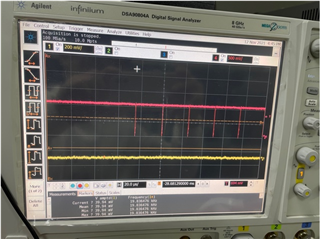
    Now I mapped VSYNC to GPIO2, I can see pulse on GPIO2. But there is also nothing display on panel. The status registers 0xf0 and 0xf1 stayed as 0x00.

    Do you have any idea I can debug on?

    thanks and best regards,

    chaodong 

  • Chaodong

    What is the frequency for the VSYNC and HSYNC? Do they match with the resolution?

    Thanks
    David

1 2