Part Number: DP83867IS
Hi all
Would you mind if we ask DP83867IS?
This thread is relation to following forum.
https://e2e.ti.com/support/interface-group/interface/f/interface-forum/1048227/dp83867is-phy-address-setting-with-strap-pins
"Please update when scope captures are available of bad reset."
"This will help determine what exactly is going one when the PHY straps into a different address during that 1 out of 400 reoccurrence. "
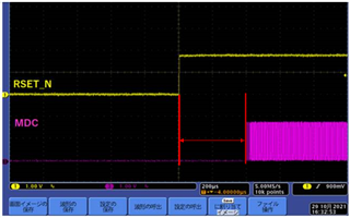
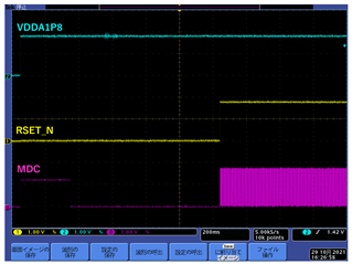
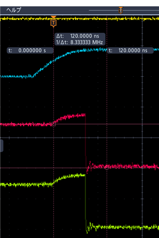
->The customer could capture bad condition and normal condition. Could you refer to the following file?
20211220_DP83867.pdf
<Question1>
There is no difference between no problem case and problem case.
-problem case : 296mV
-no problem case : 288mV
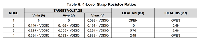
The voltage is within from 0.140 × VDDIO to 0.191 × VDDIO at both case.
Just before fixed of strap setting, it seems that pin's voltage raises.
Why does the voltage raise? Because of SGMII interface, there is no packet.
And these pins have only Mode2 resistor.
Because of transition timing(from strap pin to clkout pin), does the voltage raise at the moment?
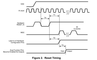
<Question2>
When does the device operate sampling of strap setting?
<Question3>
If you have EVM, could you confirm with EVM?
Kind regards,
Hirotaka Matsumoto