This thread has been locked.

If you have a related question, please click the "Ask a related question" button in the top right corner. The newly created question will be automatically linked to this question.

DS90CF384A: PCB Guidelines

Part Number: DS90CF384A
Other Parts Discussed in Thread: FLINK3V8BT-85

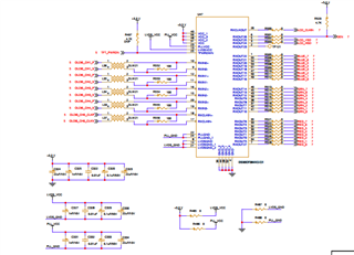
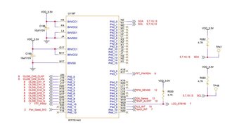
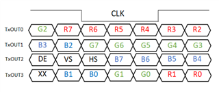
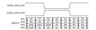
Below are the queries on DS90CF384AQ-Q1,

1. Does RGB output requires RX out resistor? if yes kindly share the resistor value.
2. Does RGB output essentially requires Length matching?
3. Does RGB output requires 50-ohm impedance trace?
4. Please share the PCB design files for routing reference

  • Hi Arun,

    1. Does RGB output requires RX out resistor? if yes kindly share the resistor value?
      1. Yes. The resistors are needed on the receiver side; therefore, you do not need to place here.
    2. Does RGB output essentially requires Length matching?
      1. Yes. OLDI/RGB is requires length match.
    3. Does RGB output requires 50-ohm impedance trace?
      1. Yes
    4. Please share the PCB design files for routing reference
      1. This device is a long time released device. I need sometime to look into this if there is any EVM design file.

    Aaron

  • We are using DS90CF384AQ-Q1 receiver,kindly suggest termination resistor value for RGB data line.  Is there a preferred placement of termination resistor?.

  • Please find the attached schematics and review the same

  • Dear Aaron,

    Please verify the pin mapping in the above-attached schematics. We are using the IC DS90CF384AQ for converting LVDS signals from the processor to RGB signals to LCD. We have followed the pin mapping from the document  SNLA014A (Table 1). confirm the pin mapping is correct for the mentioned application.

    Kindly share the design files.

  • Hi Arun,

    • Is there a preferred placement of termination resistor?
      • The termination resistor should be at the receiver side (LCD panel) not at the transmitter (DS90CF384AQ-Q1).

    Can you send me the schematic in pdf? It is too blurry to read the pinout when I zoomed in.

    Aaron

  • Thanks for the reply, Aaron.

    1. Please verify the pin mapping in the attached schematics. We are using the IC DS90CF384AQ for converting LVDS signals from the processor to RGB signals to LCD. We have followed the pin mapping from the document  SNLA014A (Table 1). confirm the pin mapping is correct for the mentioned application. 

    2. kindly review the schematics

    3. Need termination resistor value in ohms

    4. Need design files for routing reference

    5. I have connected the LCD standby pin directly to the MCU without using DS90CF384AQ. Is this correct?

    Pin Mapping Verfication.pdf

  • Hi Arun,

    Thank you for sharing the file. I will get back with you by Monday, 2/7.

    Aaron

  • Hi Aaron,

    A kind reminder of the below queries

    1. Please verify the pin mapping in the attached schematics. We are using the IC DS90CF384AQ for converting LVDS signals from the processor to RGB signals to LCD. We have followed the pin mapping from the document  SNLA014A (Table 1). confirm the pin mapping is correct for the mentioned application. 

    2. kindly review the schematics

    3. Need termination resistor value in ohms

    4. Need design files for routing reference

    5. I have connected the LCD standby pin directly to the MCU without using DS90CF384AQ. Is this correct?

    Thanks

    Arun

  • Hi Arun,

    1. Please verify the pin mapping in the attached schematics. We are using the IC DS90CF384AQ for converting LVDS signals from the processor to RGB signals to LCD. We have followed the pin mapping from the document SNLA014A (Table 1). confirm the pin mapping is correct for the mentioned application.
      • I reviewed the pin mapping. It looks good to me. According to the schematic, the pin mapping is configured for JEIDA/Format 1. It depends on the connected panel, you need to make sure that the LCD is able to accept the format 1.
    2. kindly review the schematics
      • It looks fine.
    3. Need termination resistor value in ohms
      • The termination resistor should be 100Ω on for the LVDS Rx input. You do not need to place any termination resistor on the parallel RGB side.
    4. Need design files for routing reference
      • Unfortunately, we do not have any EVM specifically for 384A. However, the FLINK3V8BT-85 is for 385A, and it should be compatible with 384A if you want to swap them out.
      • Design fileSV600605_Source.zip
      • Gerber fileSV600605_Gerber.zip
    5. I have connected the LCD standby pin directly to the MCU without using DS90CF384AQ. Is this correct?
      • Are you referring to PWRDWN pin of the 384A? If it is, I don't think it is a problem. It should be fine.

    Hope this helps. Let me know if you have further questions.

    Aaron

  • Dear Aaron,

    Thanks for the reply.

    Regarding pin mapping, I have attached the RGB-LCD datasheet. There is no such information Jeida/Vesa format available in the datasheet. I request you to check the attached datasheet of LCD and let us know whether we can use the same pin mapping for this LCD.

    Thanks

    Arun

    TM050RDZG03-00 V5.0.pdf

  • Hi Arun,

    Let me review the datasheet. I will get back with you tomorrow.

    Aaron

  • Hi Arun,

    I checked the specs of the panel. It is a RGB panel. The JEIDA and VESA format is only for LVDS mapping. The LVDS mapping is depended on the TX side in order to connect a proper RGB signal. If the incoming format from the TX side is JEIDA, then your connection is correct.

    Hope this helps. Let me know if you have further questions.

    Aaron

  • Hi Aaron,

    In this design, the processor is the TX board. The LVDS output of the processor is connected to  DS90CF384AQ-Q1, which converts LVDS to RGB signals for the RGB LCD interface. Since I am new to this design, please specify now, where can I check for the JEIDA format?

    Arun

  • Hi Arun,

    You need to check with your SoC vendor as it is not allowed me to download the datasheet.

    Aaron

  • Hi Aaron,

    Please find the attached datasheet ( LVDS section) for the processor, kindly let us know whether we can use the same pin mapping for this RGB LCD using DS90CF384AQ converter.5277.Processor LVDS section.pdf

  • Hi Aaron,

    Please find the attached datasheet ( LVDS section) for the processor, kindly let us know whether we can use the same pin mapping for this RGB LCD using DS90CF384AQ converter.5277.Processor LVDS section.pdf 

  • Hi Arun,

    Thank you for sharing the specs. I need time to look into this, and I will get back with you on 2/14.

    Aaron

  • Hi Arun,

    I reviewed the datasheet. It looks like it supports both JEIDA and VESA format. All you need to make sure is the LVDS mapping matches MCU's format. You can choose MODE 0 or MODE 4 for your display.

    Hope this helps. Let me know if you have further questions.

    Aaron