This thread has been locked.

If you have a related question, please click the "Ask a related question" button in the top right corner. The newly created question will be automatically linked to this question.

SN65LVDS93: A version vs no-A version

Part Number: SN65LVDS93

Hi Team,

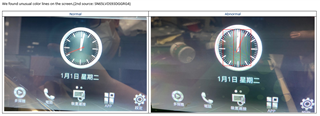
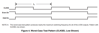
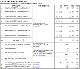
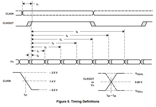
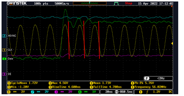
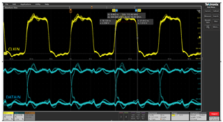
For  SN65LVDS93 A version and non-A version, I assume that they are p2p compatible. The main difference is PCLK spec. Our application PCLK = 55MHz, I think we can use both of them. But when we used non-A version, the panel pattern will be abnormal. Can you help let me know which part should we need to try?

Regards,

Roy

  • Hi Roy,

    The main difference between the SN65LVDS93 and the SN65LVDS93A version is the supported CLKIN specification, where the non-A version supports 20MHz - 68MHz and the A version supports 10MHz - 135MHz.

    If the input clock is 55MHz, then that is within the non-A device's specifications and there is no need to use the A or B versions.

    1) Could you elaborate more on what the abnormal panel display looks like?

    2) Is the pin mapping correct? Check the routing of the input and output pins of the SN65LVDS93 device.

    When you feed 28 bits into the SN65LVDS93 device, it outputs LVDS data in the format described in the "Current Cycle" in Figure 1 in the datasheet:

    3) Could you check the display datasheet and confirm that the LVDS output matches what the display expects to receive?

    Best,

    Justin Phan

  • Hi Justin,

    Please see below image.

    Regards,

    Roy

  • Hi Roy,

    It seems the pin mapping is no issue, since video is being shown, but there are unusual artifacts on some of the displays.

    1) What is the estimated failure rate (Percentage of units that show abnormal behavior)?

    2)  Could you ask the customer to probe the CLKIN signal being sent to the SN65LVDS93 device on the abnormal display? And then measure the following parameters, as defined in the datasheet?

    3) Could you also ask the customer to probe the collect as much data as possible, mentioned in the Switching Characteristics table in the datasheet? And try their best to replicate the accompanying figures in the datasheet?

    This device is relatively simple, with no register settings, so the issue may be that some spec in the datasheet is not met in the abnormal display. If the customer can share the scope screenshots or summarize the data in a table, then I can help analyze the data.

    4) Is it also possible to share the schematic of the connections made to the SN65LVDS93 device? I can look it over and try to find any anomalies. If you are not comfortable sharing the schematics over the public forum, then you can email it to me.

    Best,

    Justin Phan

  • Hi Justin,

    1.Fail rate was 100%(5/5)when we used 2nd source:SN65LVDS93DGGRG4.

    2.We found the type of clock trigger data was falling edge, but CLKSEL was rising edge. And so we set CLKSEL from rising edge to falling edge and the issue could be fixed.

    Why we didn't meet the issue in A-version. 

    Yellow:Clock input

    Green:Data

    schematic

    Roy

  • Hi Roy,

    Since abnormalities appear at a 100% rate with the SN65LVDS93, then it seems this is a configuration error instead of a part quality error.

    I recommend verifying with the customer if the video source (processor) is programmed to send parallel video data corresponding to the falling edge or rising edge of the clock signal. Our SN65LVDS93 device's CLKSEL pin needs to be configured to match the video source's sampling clock setting (rising edge or falling edge).

    In the schematic, make sure that only one of the pull-up resistors at Pin 17 are populated, such that CLKSEL is HIGH or LOW.

    The reason why using the SN65LVDS93A part works when rising edge is selected, might just be a coincidence. Skew and individual differences in parts might coincidentally meets the setup time and hold times required by the device and cause the right bits to be sampled.

    But it seems the processor is sending data corresponding to the falling edge of the clock signal, so the SN65LVDS93 device should be configured for falling edge clock, for normal operation across all devices.

    Best,

    Justin Phan

  • Hi Justin,

    Thank you for your assistance, here have a few questions:


    1. What is the specification of t7 in SN65LVDS93A?
    2. Is there any difference between t7 specification of SN65LVDS93A and SN65LVDS93 definition and system usage method?
    3. As above, although the HW CLKSEL setting is wrong, the SN65LVDS93A trigger data is normal. Is the t7 specification whether for the main reason?


    2)  Could you help probe the CLKIN signal being sent to the SN65LVDS93 device on the abnormal display? And then measure the following parameters, as defined in the datasheet?

    3) Can you help probe the collect as much data as possible, mentioned in the Switching Characteristics table in the datasheet? And try your best to replicate the accompanying figures in the datasheet?

    Answer:

    SN65LVDS93:

    Regards,

    Roy

  • Hello Roy,

    1. In the SN65LVDS93A datasheet, t7 is half the CLKIN period +/-0.1ns.
      1. Here is an E2E thread that goes in more detail: 
      2. https://e2e.ti.com/support/interface-group/interface/f/interface-forum/475010/sn65lvds93a-t7-time?tisearch=e2e-sitesearch&keymatch=SN65LVDS93a%2520t7#
    2. t7 in the A and non-A version describe completely different things. t7 in the non-A version describes the CLKIN delay time from the CLKIN rising/falling edge to the rising CLKOUT edge. The parameters in the two different datasheets do not have a direct relationship.
    3. The figure that is shown compares CLKIN to the output parameters. If the CLKIN and input data signals meet datasheet specs, then I expect the output clock and data to meet datasheet specs as well. As a result, it is important to first verify that the input signals meet datasheet specs, and then verify that the output signals match what is expected.

    Have you measured the CLKIN and Dn parameters for the SN65LVDS93 device?

    Best,

    Justin Phan

  • Hi Justin,

    Because the input data and clock are the same, we guess whether the SN65LVDS93A IC has no problem in the application due to the different t7 specification.

    what do you think?


     Have you measured the CLKIN and Dn parameters for the SN65LVDS93 device?

    [Roy]: Yes, Both are the same CLKIN and Dn on input terminal of SN65LVDS93A and SN65LVDS93.

    Regards,

    Roy

  • Hi Roy,

    The t7 parameter describes different things in the non-A and A version of the device datasheets. In the non-A version, t7 is the CLKIN to CLKOUT delay time. In the A version, t7 is half the CLKIN period. The CLKIN to CLKOUT delay time is not explicitly defined in the A version of the device datasheet, but I would expect that value to be between 4-5ns.

    From the oscilloscope screenshot, it seems that the falling edge trigger of CLKIN is the appropriate setting, since it seems t_su and t_hold are being met. Your customer may have gotten the rising edge CLKIN trigger to work in the A version by chance, where the margin of the device allowed the t_su and t_hold specifications to be met in the system that was tested. But in order to get consistent results across all systems developed, I recommend configuring CLKIN to trigger at the falling edge.

    Best,

    Justin Phan