This thread has been locked.

If you have a related question, please click the "Ask a related question" button in the top right corner. The newly created question will be automatically linked to this question.

SN65HVD234: what is the meaning of the parameter in the datasheet

Part Number: SN65HVD234

hi TI member

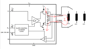
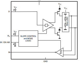
-1: when D=0 or D=VCC ,how the Driver operates?   does it operate by controling the current through the FET  ?

      -When D=0 , current through FET is high ,When D=VCC , current through FET is small,is it right ?

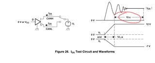
2:as reading the datasheet of SN65HVD234;

the parameter of  IOH and  IOL  , I can't understanding it , pls 

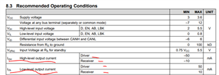
--- high level or low level is meaning of  the TXD signal ot others ? 

--does the current is meaning of the VCC Power consumption  or the Driver Power consumption ?

-- why the current is 50mA ,is it controlled by the IC internally ?

--when high-level ,why  output current is negative (-50mA)?

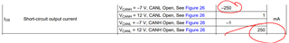
3:why list the IO of receiver output current here , is it a important parametre ?

thanks

  • Hello,

    1. When D is sitting high (VCC) the bus (CANH and CANL) sitting at the recessive level. The bias unit that you see generates this recessive level and it is equal to VCC/2.

    When D is sitting low (at GND), CANH goes high and CANL goes low creating a differential voltage between the pins. This is known as a dominant signal.

    2. This is the output current of the device when it is driving high or low. The "driver" in this case is the bus pin drivers. The "receiver" is the R pin otherwise known as the RXD pin. This is essentially telling you the strength of the these drivers.

    The high level and low level relates to the output of the pin. If it is outputting a logic high or a logic low.

    The 50 mA current relates to the strength of the FET.

    When the output is high the direction of the current changes. Remember that when you are driving a voltage there is always a voltage drop that is related to current and resistance. So if the output pin is the high level then the voltage drop is going from our pin to a lower voltage level somewhere else. So the current is leaving our device.

    3. Everything that is listed in the ABS max rating of our datasheet is important. If any of those specifications are violated then you could do permanent damage to the device.

    Best,

    Chris

  • Thanks for reply 

    -1: But about this sentense   "The 50 mA current relates to the strength of the FET.",

    I also have some doubt: ---if the strength of FET is 50mA ,why  the IOS-short-circuit output current can reach  250mA ???

    -2: when D is sitting low, CANH goes high and CANL goes low;

      how much current flow out from VCC, when the  load switch to 120Ω  or  60Ω  or  30Ω , is there some formula to get that  ?

    plz ~~

  • CAN drivers are designed to generate a voltage drop of nominally 2 V over the 60 Ω load (two 120 Ω termination resistors in parallel). There are no specifications for other loads.

    The short-circuit current is measured in the case when the output is no longer able to generate a usable voltage drop.

  • thanks

    1-I just want to konw  if three or four 120 Ω termination resistors in parallel,  how about the voltage drop will be ??  

       in some application , i used four CAN device ,every device has 120Ω termination resistor, so the equal resistor is 30Ω , the communication is ok;  

       but  the voltage drop is down to 1.2V , so I want to konw  the why the voltage drop change , and the which principle it is??

    2- ahout short circuit

      I just want to kown whether short current  flow through the FET  ??  if flows , the FET strength is 50mA ,why it can reach 250mA ,  does it depend on the time ?

    thanks

  • More resistors in parallel reduces the total resistance. There is no guarantee for higher output currents. There should be exactly two termination resistors, at the two ends of the bus.

    A MOSFET behaves similar to a resistor. (Not exactly, see figures 4 and 5.) When increasing the current, the voltage drop over the transistor increases, so there is less voltage available for the load.

  • To add onto what Clemens is saying,

    I did not use the right language in my original post so sorry for any confusion. We are talking about two different things here. What I brought up is a recommended condition of the driver. It is the maximum load that you can apply to your driver in order for the device to preform optimally. The short circuit current that you are talking about is an electrical characteristic of the driver.

    The electrical characteristic of the device is just pointing out how strong the FET is under certain loading conditions. It does not mean that you should run your device under those conditions because you could be harming the reliability and lifetime of the device. 

    Now, all of our CAN drivers are designed to drive a 60 ohm load. You can see that when we define the characteristic of our driver's differential output voltage:

    We define it using a 60 ohm load. As your load reduces the amount of current that your driver can sink becomes reduced and you will not output as large of a differential voltage. When your driver is trying to drive a voltage across a resistor it can only sink so much current and therefore you will see a smaller voltage drop with a smaller resistor. That is why when you use an equivalent 30 ohm load with 4 transceivers your differential voltage is so small.

    Make sure that only the two transceivers farthest away from each other have a 120 ohm resistor. The total resistance of your bus should be 60 ohms in order to match the characteristic impedance of your transmission line.

    Best,

    Chris