This thread has been locked.

If you have a related question, please click the "Ask a related question" button in the top right corner. The newly created question will be automatically linked to this question.

TPD4E001: DSP pin protection circuit

Part Number: TPD4E001
Other Parts Discussed in Thread: STRIKE

Hi Team,

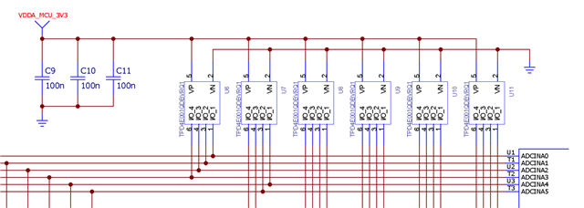
In our C2000 evaluation kit, TPD4E001 is used as the protection circuit on DSP's ADC pin, ADC pin's absolute maximum rating is 4.6V.

I am wondering when transient event happens on ADC pin nodes, how will TPD4E001 work?

TPD4E001's Vbr is 11V, which is higher than ADC pin's maximum rating, does it mean that the transient energy will conduct through the high side internal diode to VCC rather than to GND?

Does it mean that the ADC pin voltage will clamp to VCC+ Vforward(0.6V)?,

Please let me know if my understanding is correct, thanks.

  • Hi Charles,

    If the VCC pin is connected to the system power supply, the TPD4E001 works as a transient suppressor for any signal swing above VCC + VF. A 0.1-μF capacitor on the device VCC pin is recommended for ESD bypass.

    The clamping voltage in the datasheet was only specified at maximum value with a Vcc = 5 V and an ambient temperature of 25 C so the values would be slightly different with a Vcc = 3.3 V. 

    For an 8kV ESD strike (transient event), the max clamping voltage will be Vcc + 25 V. The clamping voltage is the voltage the protected IC will see.

    Note that this voltage is taken at about 30nS after an initial ESD pulse. The voltage is higher than the ABS max for the ADC pin however the duration of the pulse is very short so as long as the current rating of the DSP is not violated it shouldn't be damaged. Also note that this is maximum value, the typical clamping voltage should be much lower. 


    Regards,

    Sebastian