This thread has been locked.

If you have a related question, please click the "Ask a related question" button in the top right corner. The newly created question will be automatically linked to this question.

DS90UB954-Q1: MIPI data disappeared

Part Number: DS90UB954-Q1

Hi Sir,

My customer found the MIPI data will be disappeared between 954 and ISP SoC, how to fix this issue? please advise some comments. Thanks!
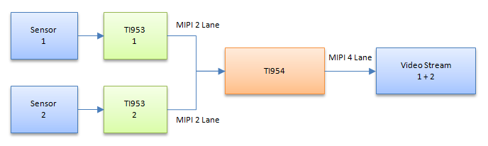
MIPI waveforms:

MIPI 4 lane waveforms for 954 to ISP SoC.docx

  • Hello Henry,

    Can you please help me understand your system/issue better by answering the below questions?

    1) On how many systems are you seeing this issue? Is it easily reproduceble?

    1) Provide the resolution, blanking, frame rate and data type from each Sensor.

    2) In which clocking mode are the SER and DES running? Is this Synchronous mode or non-Synchronous mode?

    3) What is the External Clock value on the DES? And on the SER, if any?

    4) What are the output settings of the DES? i.e. number of lanes, speed of lanes, type of port forwarding?

    5) Can you provide register dump from the DES in a good case and from a issue case?

  • Hi Sir,

    The answer as below:

    1) On how many systems are you seeing this issue? Is it easily reproducible?

    --> It is easily reproduction, the fail rate is around 10~30%.

    2) Provide the resolution, blanking, frame rate and data type from each Sensor.

    --> The sensor outputs 1280x720 30fps by MIPI 2 lanes.

    3) In which clocking mode are the SER and DES running? Is this Synchronous mode or non-Synchronous mode?

    --> We set dual sensor in synchronous mode.

    4) What is the External Clock value on the DES? And on the SER, if any?

    --> There is a 25MHz crystal on DES.

    5) What are the output settings of the DES? i.e. number of lanes, speed of lanes, type of port forwarding?

    --> 4 lanes output and 800MHz per lane.

    6) Can you provide register dump from the DES in a good case and from a issue case?

    --> I checked the registers of two cases are the same, and the setting shown as below.

    DES register dump :

    TAG:00
    
    7A 01 02 ;reset all
    ;SL 200
    SL 150
    
    7A 0c cf
    ;7A 10 91
    7A 10 90	;GPIO0 input
    7A 11 85
    7A 13 89
    7A 14 8d
    7A 19 15
    7A 1a b3
    7A 1b c3
    7A 1c 4F
    ;7A 18 01	;enable FSIN
    7A 18 00	;disable FSIN
    
    7A 4c 01	;SELECT PORT0
    7A 58 5e	;Enable I2C Pass Through
    7A 5c 30	;Serializer Alias
    7A 5d 78	;native I2C ID
    7A 65 78	;Imager alias
    7A 6F 00	;0A	;BCC GPIO2 select frame sync signal
    7A 6E 00	;0A
    7A 70 2B 	;RAW10 DT + VC0
    7A 71 2C 	;RAW12 DT + VC1
    7A 72 E4 	;VC Mapping default - vc0
    
    7A 4c 12	;SELECT PORT1
    7A 58 5e	;Enable I2C Pass Through
    7A 5c 32	;Serializer Alias
    7A 5d 78	;native I2C ID
    7A 65 7C	;Imager alias
    7A 6F 00	;0A	;BCC GPIO2 select frame sync signal
    7A 6E 00	;0A
    7A 70 6B 	;RAW10 DT + VC0
    7A 71 6C 	;RAW12 DT + VC1
    7A 72 fe 	;VC Mapping default - vc1
    
    7A 32 01
    7A 33 03	;CSI Continous clock + 4 Lanes
    SL 2
    7A 20 00	;Forward all RX to CSI0
    SL 2
    
    30 0e 90	;[7:4]: enable GPIO0/1/2/3 output
    ;30 0d 30	;enable FSIN remote control 
    30 0d 10	;20
    SL 2
    ;30 0d 38
    30 0d 18	;28
    30 0b 20	;I2C speed: 390K
    30 0c 20
    30 02 53	;MIPI 2lane; 73: 4lane
    ;30 06 43	;refclk to sensor:24MHz
    ;30 07 7D
    
    32 0e 90	;[7:4]: enable GPIO0/1/2/3 output
    ;32 0d 30	;enable FSIN remote control 
    32 0d 10	;20
    SL 2
    ;32 0d 38
    32 0d 18	;28
    32 0b 20	;I2C speed: 390K
    32 0c 20
    32 02 53	;MIPI 2lane; 73: 4lane
    ;32 06 43	;refclk to sensor:24MHz
    ;32 07 7D
    

    .

  • Hello Henry,

    I am looking through this and will get back to you.

  • Hello Henry,

    I have reviewed your configurations in the provided Word file, and here is my feedback. In many positions these settings make no sense!!

    Serdes setting for 953 and 954:

    TAG:00

     7A 01 02 ;reset all

    ;SL 200

    SL 150


    7A 0c cf – Writing Reserved bit [6] default 0 to 1.

    ;7A 10 91

    7A 10 90          ;GPIO0 input – Not required since default is output disabled!

    7A 11 85 – GPIO1 is used for Rx Port1 LOCK indication

    7A 13 89 – GPIO3 settings invalid!

    7A 14 8d – GPIO4 settings invalid!

    7A 19 15 -

    7A 1a b3

    7A 1b c3

    7A 1c 4F

    ;7A 18 01         ;enable FSIN

    7A 18 00          ;disable FSIN - – Not required since default is FSync disabled!

     7A 4c 01          ;SELECT PORT0

    7A 58 5e          ;Enable I2C Pass Through

    7A 5c 30          ;Serializer Alias

    7A 5d 78          ;native I2C ID

    7A 65 78          ;Imager alias

     7A 6F 00          ;0A       ;BCC GPIO2 select frame sync signal – With setting this register to 00, you are sending the data from DES GPIO0 to the SER GPIO3, and sending the data from DES GPIO0 to the SER GPIO2

     7A 6E 00          ;0A – With setting this register to 00, you are sending the data from DES GPIO0 to the SER GPIO1, and sending the data from DES GPIO0 to the SER GPIO0

     7A 70 2B          ;RAW10 DT + VC0

    7A 71 2C          ;RAW12 DT + VC1  not required, since you are not using DVP

    7A 72 E4          ;VC Mapping default - vc0 – not required since default

     7A 4c 12          ;SELECT PORT1

    7A 58 5e          ;Enable I2C Pass Through

    7A 5c 32          ;Serializer Alias

    7A 5d 78          ;native I2C ID

    7A 65 7C          ;Imager alias

     7A 6F 00          ;0A       ;BCC GPIO2 select frame sync signal - – With setting this register to 00, you are sending the data from DES GPIO0 to the SER GPIO3, and sending the data from DES GPIO0 to the SER GPIO2

     7A 6E 00          ;0A - – With setting this register to 00, you are sending the data from DES GPIO0 to the SER GPIO1, and sending the data from DES GPIO0 to the SER GPIO0

     7A 70 6B          ;RAW10 DT + VC0

    7A 71 6C          ;RAW12 DT + VC1 - not required, since you are not using DVP

    7A 72 fe           ;VC Mapping default - vc1 – Configure to 55 instead of FE

     7A 32 01 – reg 0x32 is reserved. Please do not write!!

    7A 33 03          ;CSI Continous clock + 4 Lanes

    SL 2

    7A 20 00          ;Forward all RX to CSI0 – Move out setting reg 0x33 and 0x20 till the end, after configuring the SER and the Image sensor.

    SL 2

     30 0e 90          ;[7:4]: enable GPIO0/1/2/3 output – You are enabling only GPIO0 and 3 as outputs.

    ;30 0d 30         ;enable FSIN remote control

    30 0d 10          ;20 – You are enabling DES GPIO0 on local GPIO0 !!

     SL 2

    ;30 0d 38

    30 0d 18          ;28 – You are enabling DES GPIO0 on local GPIO0, and setting local GPIO3 to 1 !!

     30 0b 20          ;I2C speed: 390K

    30 0c 20

    30 02 53          ;MIPI 2lane; 73: 4lane

    ;30 06 43         ;refclk to sensor:24MHz

    ;30 07 7D -  To avoid higher jitter on the generated CLKOUT, it is recommended to set reg 0x06 to 0x41, and reg 0x07 to 0x2A. But you will be getting CLKOUT of 23.81MHz instead of 24MHz

     32 0e 90          ;[7:4]: enable GPIO0/1/2/3 output

    ;32 0d 30         ;enable FSIN remote control

    32 0d 10          ;20

    SL 2

    ;32 0d 38

    32 0d 18          ;28

    32 0b 20          ;I2C speed: 390K

    32 0c 20

    32 02 53          ;MIPI 2lane; 73: 4lane

    ;32 06 43         ;refclk to sensor:24MHz

    ;32 07 7D  These are repeated settings!!

  • Hi Sir,

    Thank you for your comments, they will try to modify the configurations.

    BTW, they removed the POC power on the 953A PCB and found the system has working well.

    Could you also review the schematics and PCB layout for the PoC circuit?

    954953A_Schematics PCB:954953A_Schematics PCB.rar

  • Hello Henry,

    Yes, I will review these and get back to you within the next two days.

  • Hi Sir,

    I shared the info about the POC power is 10V-in with I-in 110mA.

    The customer tried to use your configurations, they found the video signals did not output and saw the pass and lock LEDs are normal.

    Please also refer to the below configurations file.

    TAG:00
    
    7A 01 02	;rest all
    SL 150
    
    7A 0C CF	;writing Reserved bit [6] default 0 to 1
    ;7A 10 90	;Not required since default is output disabled!
    7A 11 85	;GPIO1 is used for Rx Port1 LOCK indication
    7A 13 89	;GPIO3 settings invalid!
    7A 14 8d	;GPIO4 settings invalid!
    7A 19 15
    7A 1A B3
    7A 1B C3
    7A 1C 4F
    ;7A 18 01	;enable FSIN
    7A 18 00	;disable FSIN - – Not required since default is FSync disabled!
    
    7A 4C 01	;SELECT PORT0
    7A 58 5E	;Enable I2C Pass Through
    7A 5C 30	;Serializer Alias
    7A 5D 78	;native I2C ID
    7A 65 78	;Imager alias
    7A 6F 00	;0A	;BCC GPIO2 select frame sync signal – With setting this register to 00, you are sending the data from DES GPIO0 to the SER GPIO3, and sending the data from DES GPIO0 to the SER GPIO2
    7A 6E 00	;0A – With setting this register to 00, you are sending the data from DES GPIO0 to the SER GPIO1, and sending the data from DES GPIO0 to the SER GPIO0
    ;7A 70 2B	;RAW10 DT + VC0
    ;7A 71 2C	;RAW12 DT + VC1  not required, since you are not using DVP
    ;7A 72 E4	;VC Mapping default - vc0 – not required since default
    
    7A 4C 12	;SELECT PORT1
    7A 58 5E	;Enable I2C Pass Through
    7A 5C 32	;Serializer Alias
    7A 5D 78	;native I2C ID
    7A 65 7C	;Imager alias
    7A 6F 00	;0A	;BCC GPIO2 select frame sync signal – With setting this register to 00, you are sending the data from DES GPIO0 to the SER GPIO3, and sending the data from DES GPIO0 to the SER GPIO2
    7A 6E 00	;0A – With setting this register to 00, you are sending the data from DES GPIO0 to the SER GPIO1, and sending the data from DES GPIO0 to the SER GPIO0
    ;7A 70 6B	;RAW10 DT + VC0
    ;7A 71 6C	;RAW12 DT + VC1  not required, since you are not using DVP
    7A 72 55	;VC Mapping default - vc1 – confifure to 55 instead of FE
    
    ;7A 32 01	;reg 0x32 is reserved. Please do not write!!
    ;7A 33 03	;CSI Continous clock + 4 Lanes
    ;SL 2
    ;7A 20 00	;Forward all RX to CSI0 – Move out setting reg 0x33 and 0x20 till the end, after configuring the SER and the Image sensor.
    ;SL 2
    
    30 0E 90	;[7:4]: enable GPIO0/1/2/3 output – You are enabling only GPIO0 and 3 as outputs.
    ;30 0D 30	;enable FSIN remote control
    30 0D 10	;20 – You are enabling DES GPIO0 on local GPIO0 !!
    SL 2
    ;30 0D 38
    30 0D 18	;28 – You are enabling DES GPIO0 on local GPIO0, and setting local GPIO3 to 1 !!
    30 0B 20	;I2C speed: 390K
    30 0C 20
    30 02 53	;MIPI 2lane; 73: 4lane
    30 06 41	;43	;refclk to sensor:24MHz
    30 07 2A	;7D -  To avoid higher jitter on the generated CLKOUT, it is recommended to set reg 0x06 to 0x41, and reg 0x07 to 0x2A. But you will be getting CLKOUT of 23.81MHz instead of 24MHz
    
    32 0E 90	;[7:4]: enable GPIO0/1/2/3 output
    ;32 0D 30	;enable FSIN remote control
    32 0D 10	;20
    SL 2
    ;32 0D 38
    32 0D 18	;28
    32 0B 20	;I2C speed: 390K
    32 0C 20
    32 02 53	;MIPI 2lane; 73: 4lane
    32 06 41	;43	;refclk to sensor:24MHz
    32 07 2A	;7D  These are repeated settings!!

  • Hello Henry,

    please see my Schematic review feedback attached. 

    I could not review the layout from the PDF. Please provide Gerber files for that!

    DS90UB953A_sch_TI-Feedback.pdfDS90UB954_sch_TI-Feedback.pdf

  • Hi Sir,

    May I have your friendship request? I will provide the Gerber files by the friendship. Thanks!

    BTW, The customer follow to use your configurations, they found the video signals did not output. please help to review the configurations. Thanks!

    TAG:00
    
    7A 01 02	;rest all
    SL 150
    
    7A 0C CF	;writing Reserved bit [6] default 0 to 1
    ;7A 10 90	;Not required since default is output disabled!
    7A 11 85	;GPIO1 is used for Rx Port1 LOCK indication
    7A 13 89	;GPIO3 settings invalid!
    7A 14 8d	;GPIO4 settings invalid!
    7A 19 15
    7A 1A B3
    7A 1B C3
    7A 1C 4F
    ;7A 18 01	;enable FSIN
    7A 18 00	;disable FSIN - – Not required since default is FSync disabled!
    
    7A 4C 01	;SELECT PORT0
    7A 58 5E	;Enable I2C Pass Through
    7A 5C 30	;Serializer Alias
    7A 5D 78	;native I2C ID
    7A 65 78	;Imager alias
    7A 6F 00	;0A	;BCC GPIO2 select frame sync signal – With setting this register to 00, you are sending the data from DES GPIO0 to the SER GPIO3, and sending the data from DES GPIO0 to the SER GPIO2
    7A 6E 00	;0A – With setting this register to 00, you are sending the data from DES GPIO0 to the SER GPIO1, and sending the data from DES GPIO0 to the SER GPIO0
    ;7A 70 2B	;RAW10 DT + VC0
    ;7A 71 2C	;RAW12 DT + VC1  not required, since you are not using DVP
    ;7A 72 E4	;VC Mapping default - vc0 – not required since default
    
    7A 4C 12	;SELECT PORT1
    7A 58 5E	;Enable I2C Pass Through
    7A 5C 32	;Serializer Alias
    7A 5D 78	;native I2C ID
    7A 65 7C	;Imager alias
    7A 6F 00	;0A	;BCC GPIO2 select frame sync signal – With setting this register to 00, you are sending the data from DES GPIO0 to the SER GPIO3, and sending the data from DES GPIO0 to the SER GPIO2
    7A 6E 00	;0A – With setting this register to 00, you are sending the data from DES GPIO0 to the SER GPIO1, and sending the data from DES GPIO0 to the SER GPIO0
    ;7A 70 6B	;RAW10 DT + VC0
    ;7A 71 6C	;RAW12 DT + VC1  not required, since you are not using DVP
    7A 72 55	;VC Mapping default - vc1 – confifure to 55 instead of FE
    
    ;7A 32 01	;reg 0x32 is reserved. Please do not write!!
    ;7A 33 03	;CSI Continous clock + 4 Lanes
    ;SL 2
    ;7A 20 00	;Forward all RX to CSI0 – Move out setting reg 0x33 and 0x20 till the end, after configuring the SER and the Image sensor.
    ;SL 2
    
    30 0E 90	;[7:4]: enable GPIO0/1/2/3 output – You are enabling only GPIO0 and 3 as outputs.
    ;30 0D 30	;enable FSIN remote control
    30 0D 10	;20 – You are enabling DES GPIO0 on local GPIO0 !!
    SL 2
    ;30 0D 38
    30 0D 18	;28 – You are enabling DES GPIO0 on local GPIO0, and setting local GPIO3 to 1 !!
    30 0B 20	;I2C speed: 390K
    30 0C 20
    30 02 53	;MIPI 2lane; 73: 4lane
    30 06 41	;43	;refclk to sensor:24MHz
    30 07 2A	;7D -  To avoid higher jitter on the generated CLKOUT, it is recommended to set reg 0x06 to 0x41, and reg 0x07 to 0x2A. But you will be getting CLKOUT of 23.81MHz instead of 24MHz
    
    32 0E 90	;[7:4]: enable GPIO0/1/2/3 output
    ;32 0D 30	;enable FSIN remote control
    32 0D 10	;20
    SL 2
    ;32 0D 38
    32 0D 18	;28
    32 0B 20	;I2C speed: 390K
    32 0C 20
    32 02 53	;MIPI 2lane; 73: 4lane
    32 06 41	;43	;refclk to sensor:24MHz
    32 07 2A	;7D  These are repeated settings!!

  • Hello Henry,

    In my last review for your script, I have provided some corrections and comments indicating wrong settings. In your latest script I can see same errors are still present! It looks like you have just copied my comments without correcting the errors I have pointed out!

    Please read all my comments on the script review and correct all these errors!

  • Hi Sir,

    OK, the customer will re-check the settings again, may I send the Gerber files to you go through the private e-mail address?

  • Please let them try changing the settings as suggested. If that does not help, then you can send me the layout for review.