This thread has been locked.

If you have a related question, please click the "Ask a related question" button in the top right corner. The newly created question will be automatically linked to this question.

TIC10024-Q1: Failure Modes of Contact monitor used in our BCM

Part Number: TIC10024-Q1

Hi,

I'm the hardware engineer working on Part 5 of ISO-26262. I'm doing the analysis of the effects of random hardware failures, and I need some clarification of some failure modes included in the safety documentation of the TIC10024QDCP*Q1.
The failure modes are:

  • Monitoring System and Protection Error
  • Logic Blocks and Clock Failure
  • Communication Error

What are the exact effects of each failure mode?

Additionally, in which failure mode is included a failure of the wetting current?

Best regards and thanks in advance,


Alexis

  • Hi Alexis,

    • Monitoring System and Protection Error
      • This would be a failure of the Input pin monitoring and ESD protection circuits that if damaged could lose the ability to monitor the switch connected to that Input pin.  Wetting current failure would best fall within this category.
    • Logic Blocks and Clock Failure
      • This would be a failure in the digital logic block associated with the internal state machine and clock oscillator circuit that could prevent proper timing and state change functions.
    • Communication Error
      • This would be a failure that would impact SPI communication.

    Regards,

    Jonathan

  • Hi Jonathan thanks!

    One last thing following this topic, the failure of the digital blocks would affect somehow the SPI? and the MCU could detect it?

  • Hi Alexis,

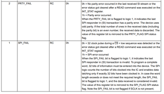
    The SPI block uses a Parity Bit as part of the transaction that can be used to detect an error in the bit sequence that "could" come as a result of some sort of device failure which will generate an interrupt to the MCU.  Also, the SPI block counts the number of clock pulses during a SPI transaction to ensure there are is exactly 32 clock pulses (or bits).  An incorrect number of clock pulses or data bits would be a failure and this could also be an indication of a SPI failure which will also generate an interrupt to the MCU.

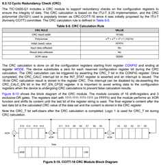
    The device also uses a CRC calculation on all the writable configuration registers.  When a CRC calculation is initiated, all of the device registers are run through the CRC calculation procedure and the result can be read back and verified by the MCU.  If any of the register bits have changed, the CRC value will be different than expected and the MCU can know that there is a problem with the integrity of the device's configuration and it may have become corrupted and need to be re-configured. 

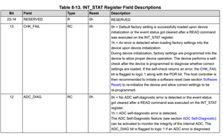
    The device will also check that the factory default values were successfully loaded at the device initialization.  If this fails, it could be an indication of a device failure and generate an interrupt to the MCU.  Also, the ADC also has a self-diagnostic test that can be used to determine if the ADC is accurate and working properly.  This can also be periodically monitored by the MCU and generate an interrupt.

    Regards,

    Jonathan