This thread has been locked.

If you have a related question, please click the "Ask a related question" button in the top right corner. The newly created question will be automatically linked to this question.

TUSB214-Q1: Please review the schematic, and have a question

Part Number: TUSB214-Q1
Other Parts Discussed in Thread: TUSB214

Dear TI experts,

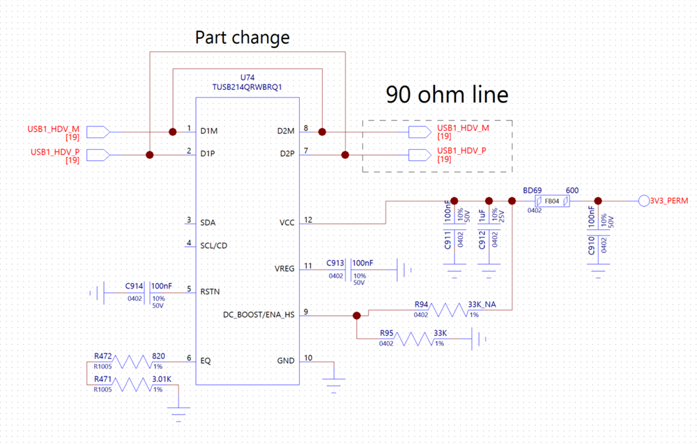
My customer made their PCB with TUSB214-Q1.

Actually they tested with TUSB214 EVM, and they drew the schematic just like they tested with EVM.

(I posted E2E thread while testing.)

https://e2e.ti.com/support/interface-group/interface/f/interface-forum/1214250/tusb214-q1-please-review-the-schematic-and-have-some-question

but the sample do not working now. Could you review the schematic first?

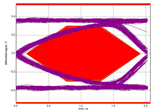
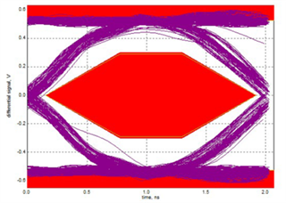
the diagram below is not applying TUSB214.

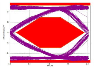
the diagram below is applying TUSB214.

and here are the questions.

1. last time I found that VCC should be applied first before USB communication is started. (TUSB214 does now work if USB communication start first.)

Is there any minimum time between applying VCC and start USB communication?

2. if USB memory attached, SCL is 3.3V and SDA is 2.8V. but if I remove USB drive, SCL and SDA is 0V.

Is it related to not-working situation?

Please check this issue. Thanks.

Best regards,

Chase

  • Hi Chase,

    (TUSB214 does now work if USB communication start first.)

    TUSB214-Q1 just shows the power on even USB host Vbus is connected, but the compensation of TUSB214-Q1 is not featured at this time. To power with compensation features for TUSB214-Q1, you need to follow these sequence.

    1. Apply Vcc
    2. Apply USB Host Vbus
    3. Applied Device high speed port

    For I2C mode, you need 4.7k ohm pull-up resistor to Vcc for SDA and SCL pins each, but the schematic doesn't show the resistors on the pins. Could you clarify that you are using on I2C mode or non-I2C mode? Have you passed USB TX compliance testing (sending Test_Packet pattern via text fixture)? And which AC boost and DC boost setting are you using?


    Best,

    Josh

  • Dear Josh,

    Thank you for your support.

    1. My customer uses non-I2C mode. I thought that I just left floating SCL and SDA if I use non-I2C mode.

    2. I don't know they tested USB TX compliance test. I will ask it to my customer.

    3. they use AC boost level 2 (3.83K) and 40mV low DC boost (33K pull up)

    the question is why this schematic does not work even the EVM is working. Can you guess the point of difference?

    Best regards,

    Chase

  • Hi Chase,

    1. I don't understand why you measured the voltages of SCL and SDA pins even if it was in non-I2C mode and it is floating.
    2. If the USB TX compliance test was not passed, the eye dram is obviously not passed.
    3. We would recommend starting the redriver to the lowest setting and then incrementing the level setting until passing the test.

    To answer your question, the schematic looks good. I could say you need to check the USB TX compliance test first.

    If you follow the test procedure and have passed the compliance test, but still have an issue, we can now approach the device internally.
    However, most of the issues about eye diagram failure from customers occurred because it was not passed the compliance test, and that is why I asked you to check if the TX compliance test is passed. I couldn't approach anything before the test passed since the compliance test is the primary checklist.

    You can refer to the test procedure for the compliance test from the app note (High Speed Signal Quality Test Modes - SLLA593). Please double-check that the test fixture is connected to TUSB214-Q1 before enable the source to send the TEST_PACKET.  It might be helpful to see testing section on this app note (TUSB2XX Implementation Guide - SLLA392)

    Best,

    Josh

  • Dear Josh,

    Thank you for your support.

    we tested with AC/DC boost level 0, it had little difference. You can compare with the eye diagram with upper one.

    also I am still reviewing the schematic and layout. Could you simulate the impedance match of USB line?

    here is the stack up data and width/distance of USB line.

    PCB__Build-up_10L_E-Type_1.6T_Stack-up.xlsx

    (U74 is TUSB214-Q1, USB line width is 0.09, and USB line distance is 0.097.)

    Please check this issue. Thanks.

    Best regards,

    Chase

  • Hi Chase,

    The layout looks good.

    • Could you confirm that you sent TEST_PACKET via xHCI Electrical Test Tool as below
    • Could you share your test set up diagram

    Best,

    Josh

  • Dear Josh,

    Thank you for your support.

    My customer still do some tests for fix the problem.

    Actually they use USB protection IC, MAX20338 (ADI).

    ADI recommends inductor as filter in USB line. and they drew MAX20038 -> TUSB214-Q1 -> inductor(filter) -> USB connector.

    Do you have any idea that the sequence of TUSB214 and inductor? Because we think that MAX20028 -> inductor -> TUSB214-Q1 -> USB connector is right sequence.

    Please give me your idea about it.

    Best regards,

    Chase

  • Hi Chase,

    • Could you confirm that you sent TEST_PACKET via xHCI Electrical Test Tool as below
    • Could you share your test set up diagram

    Could you please confirm that you followed this test sequence and you were able to see that TEST_PACKET is sent?
    Before the test is set up properly, it is hard to give any suggestions or ideas from our side.

    Best,

    Josh