Part Number: DS90UB954-Q1
Dear team
Regarding of the following questions about FPD-link, Could you help to recommend?
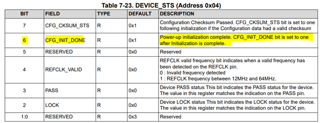
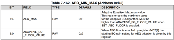
1. What is the difference between AEQ setting Full range and disable?
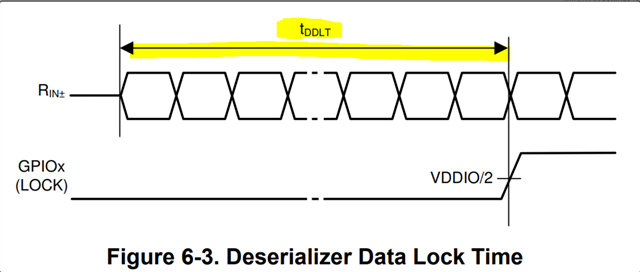
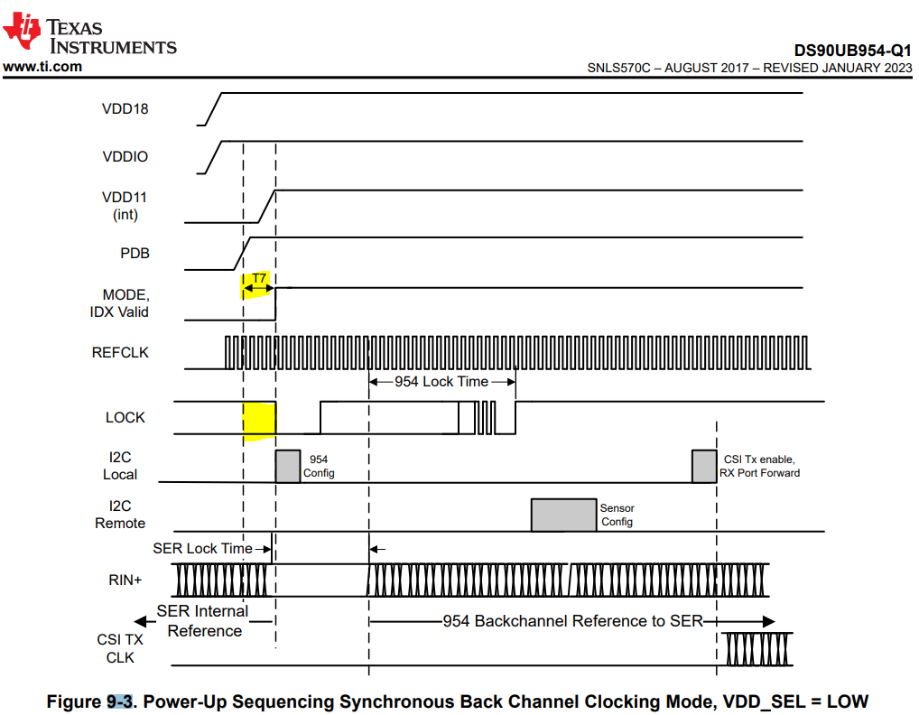
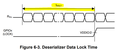
2. The current AEQ setting is Full range (set 0xD5 = 0x0E, EQ=0~14 full range). That is to say, lock out high will be after 300ms(TDDLT) at most, right?
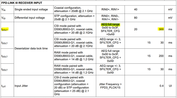
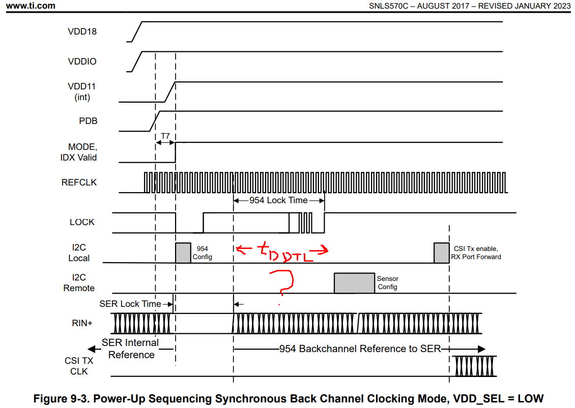
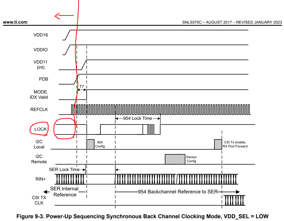
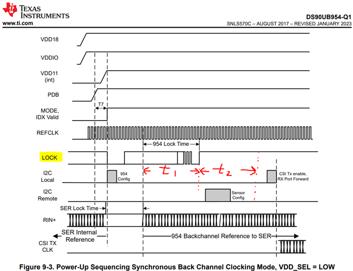
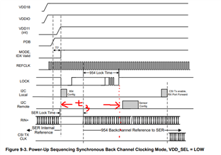
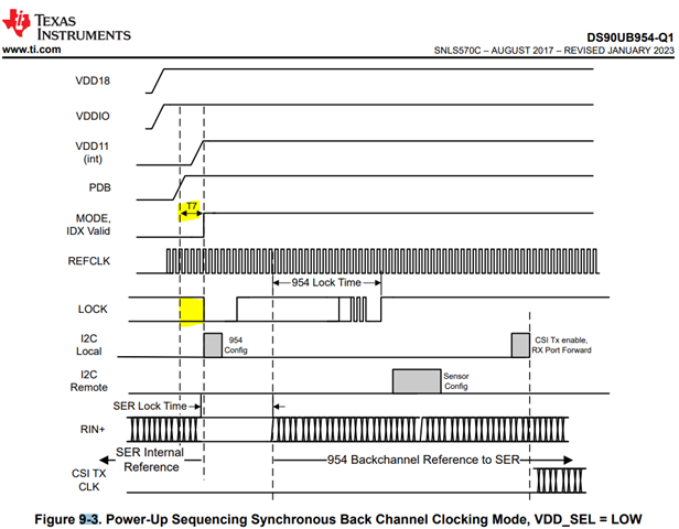
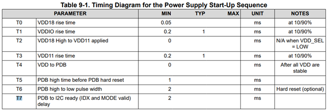
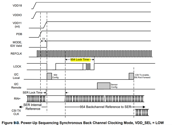
3. In 953/954 initial, how long is the lock time defined? (sync mode)
Many thanks
Denny