This thread has been locked.

If you have a related question, please click the "Ask a related question" button in the top right corner. The newly created question will be automatically linked to this question.

DS90UB936-Q1: Init sequence to receive pattern generation

Part Number: DS90UB936-Q1
Other Parts Discussed in Thread: DS90UB953-Q1EVM, DS90UB933-Q1, , ALP

Hi 

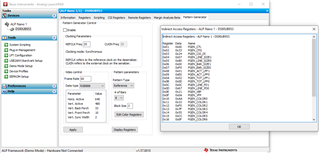
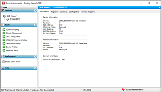
I'm trying to get a pattern generated from DS90UB953-Q1EVM.


I'm using a driver for ds90ub936-q1 for a camera that uses ds90ub933-q1 as an example.

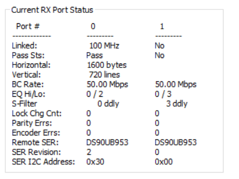
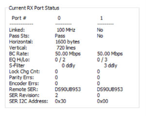
I was able to detect the EVM address and set the back channel speed to 50 Mbps, and with this the serializer is detectable. But I am unable to get the pattern from the other side.

For a camera, the init sequence is the following:

WriteI2C(0x4c, 0xf) 

WriteI2C(0x5b, 0xb0) 

WriteI2C(0x5d, 0x48) 

WriteI2C(0x4c, 0x1) 

WriteI2C(0x5b, 0xb0) 

WriteI2C(0x5c, 0xb0)

WriteI2C(0x5d, 0x48)  

WriteI2C(0x65, 0x48) 

WriteI2C(0x7c, 0x81) 

WriteI2C(0x72, 0x0) 

WriteI2C(0x70, 0x1e) 

WriteI2C(0x6d, 0x7f)

WriteI2C(0xc, 0x3) 

Most of this settings is to write the I2C address is expecting, however since I'm trying to use the pattern generation feature, I don't have a sensor. What should I write to registers 0x5d and 0x5e?

Thanks in advance,

Leonardo

  • Hi Leonardo, 

    In your system, I'm assuming the 933 and 953 are being used interchangeably. 

    In order to configure the pattern generator feature, you will need to refer to the pattern generator indirect registers. A Pattern Generator tab is available in the Analog LaunchPad GUI, where the user can input the desired video parameters and configure the pattern generator. If the registers are desired, the user can click to display registers and a box will output showing which register writes are needed. An example can be seen here: 

    Registers 0x5D and 0x5E do not need to be written to in order to configure Pattern Generator.

    An example script is as follows: 

    #first serializer enable patgen
    board.WriteI2C(serAlias1, 0xB0, 0x02) #IA_AUTO_INC=1
    board.WriteI2C(serAlias1, 0xB1, 0x01)
    board.WriteI2C(serAlias1, 0xB2, 0x01)      
    print "patgen port 0 is enabled"
    #2560x1440, 30 fps, RAW10
    board.WriteI2C(serAlias1, 0xB2, 0x35)                # PGEN_CFG
    board.WriteI2C(serAlias1, 0xB2, 0x2B)                # PGEN_CSI_DI
    board.WriteI2C(serAlias1, 0xB2, 0x03)                # PGEN_LINE_SIZE1
    board.WriteI2C(serAlias1, 0xB2, 0x20)                # PGEN_LINE_SIZE0
    board.WriteI2C(serAlias1, 0xB2, 0x00)                # PGEN_BAR_SIZE1
    board.WriteI2C(serAlias1, 0xB2, 0x64)                # PGEN_BAR_SIZE0
    board.WriteI2C(serAlias1, 0xB2, 0x01)                # PGEN_ACT_LPF1
    board.WriteI2C(serAlias1, 0xB2, 0xE0)                # PGEN_ACT_LPF0
    board.WriteI2C(serAlias1, 0xB2, 0x01)                # PGEN_TOT_LPF1
    board.WriteI2C(serAlias1, 0xB2, 0xE0)                # PGEN_TOT_LPF0
    board.WriteI2C(serAlias1, 0xB2, 0x0D)                # PGEN_LINE_PD1
    board.WriteI2C(serAlias1, 0xB2, 0x90)                # PGEN_LINE_PD0
    board.WriteI2C(serAlias1, 0xB2, 0x00)                # PGEN_VBP
    board.WriteI2C(serAlias1, 0xB2, 0x00)                # PGEN_VFP
    board.WriteI2C(desAddr,0x33,0x03) # Enable CSI-2
    board.WriteI2C(desAddr,0x20,0x20) # Forward RX0 to CSI-2 output

    Please note the exact register settings will change as dependent on the video parameters. 

    Best,

    Zoe

  • Hi Zoe,
    Yes, we are using cameras with 933 and want to use 953 to simulate those cameras using the pattern generation.

    Sorry I didn't make myself clear.

    The init sequence shown above is for the deserializer that receives the data (ds90ub936).

    I think I can generate the pattern, but it looks like the deserializer is not set to receive the data.

    What I am asking is any help to perform a init sequence for the deserializer to receive the data from the evm.

    Best Regards,

    Leonardo

  • Hello Leonardo,

    Thank you for the clarification! If the only concern currently is to configure the deserializer to receive the pattern generation, the following two register writes from the code in my previous response would be needed. 

    board.WriteI2C(desAddr,0x33,0x03) # Enable CSI-2, continuous clock mode
    board.WriteI2C(desAddr,0x20,0x20) # Forward RX0 to CSI-2 output

    The register setting for 0x20 corresponds to the RX port the pattern generation is being sent on. In this example, RX0 is the port for the 953. The initialization sequence previously shared for the 936. 

    Reviewing the initialization script provided for the DS90UB936, I have the following questions: 

    WriteI2C(0x4c, 0xf) 

    I do not suggest writing this value to F as bits 3:2 of this register are reserved. Recommend 0x2 or 0x1 to enable writes to Port 1 or Port 0, or 0x3 for both ports. 

    WriteI2C(0x5b, 0xb0) 

    WriteI2C(0x5d, 0x48) 

    WriteI2C(0x4c, 0x1) 

    WriteI2C(0x5b, 0xb0) 

    WriteI2C(0x5c, 0xb0)

    WriteI2C(0x5d, 0x48)  

    Why is 0x5c and 0x5d written to again here? 

    WriteI2C(0x65, 0x48) 

    WriteI2C(0x7c, 0x81) 

    This line here is configuring the device for Raw 10 8-bit mode

    WriteI2C(0x72, 0x0) 

    WriteI2C(0x70, 0x1e) 

    Raw 10 DT has default 0x2B to match the CSI specification. Why is 0x1E being written to here? 

    WriteI2C(0x6d, 0x7f)

    Raw 10 mode, coax overwriting straps

    WriteI2C(0xc, 0x3) 

    Since the device is in Raw10 mode, please verify Pattern Generator is sending Raw10 data as well. Specifics on what is needed for configuring Raw10 are listed in Section 7.6 Pattern Generation of the DS90UB953 datasheet. 

    Best,

    Zoe 

  • Hi Zoe,

    in regards to the initialization script provided for the DS90UB936, would this be a better initialization:

    i2ctransfer -v -f -y 10 w2@0x30 0x33 0x03    # Enable CSI-2, continuous clock mode
    i2ctransfer -v -f -y 10 w2@0x30 0x20 0x20    # Forward RX0 to CSI-2 output

    i2ctransfer -v -f -y 10 w2@0x30 0x4c 0x03    # Enable writes to Port 1 and Port 0.
    i2ctransfer -v -f -y 10 w2@0x30 0x5b 0xb0    # SER_ID -> normally loaded automatically from remote serializer
    i2ctransfer -v -f -y 10 w2@0x30 0x5d 0x48    # Configures the physical I2C address of the remote I2C Target device attached to the remote Serializer
    i2ctransfer -v -f -y 10 w2@0x30 0x4c 0x01    # Write Enable for RX port 0 registers
    i2ctransfer -v -f -y 10 w2@0x30 0x5c 0xb0    # SER_ALIAS_ID -> 7-bit Remote Serializer Alias ID
    i2ctransfer -v -f -y 10 w2@0x30 0x65 0x48    # TARGET_ALIAS_ID0 -> 7-bit Remote Target Device Alias ID 0
    i2ctransfer -v -f -y 10 w2@0x30 0x7c 0x81    # This line here is configuring the device for Raw 10 8-bit mode; FrameValid is low for the duration of the video frame
    i2ctransfer -v -f -y 10 w2@0x30 0x72 0x00    # Channel Identifier (VC-ID) of incoming CSI packets.
    i2ctransfer -v -f -y 10 w2@0x30 0x70 0x2b    # Raw 10 DT has default 0x2B to match the CSI specification.
    i2ctransfer -v -f -y 10 w2@0x30 0x6d 0x7f     # Raw 10 mode, coax overwriting straps
    i2ctransfer -v -f -y 10 w2@0x30 0x0c 0x03    # Enable Port 0 and Port 1 receiver


    i was checking the the capter "7.6.4 Code Example for Pattern Generator" from DS90UB953 datasheet which provides this example:

    #Patgen RGB888 1920x1080p30 Fixed 8 Colorbar
    WriteI2C(0xB0,0x00) # Indirect Pattern Gen Registers
    WriteI2C(0xB1,0x01) # PGEN_CTL
    WriteI2C(0xB2,0x01)
    WriteI2C(0xB1,0x02) # PGEN_CFG
    WriteI2C(0xB2,0x33)
    WriteI2C(0xB1,0x03) # PGEN_CSI_DI
    WriteI2C(0xB2,0x24) # RGB888
    WriteI2C(0xB1,0x04) # PGEN_LINE_SIZE1
    WriteI2C(0xB2,0x16)
    WriteI2C(0xB1,0x05) # PGEN_LINE_SIZE0
    WriteI2C(0xB2,0x80)
    WriteI2C(0xB1,0x06) # PGEN_BAR_SIZE1
    WriteI2C(0xB2,0x02)
    WriteI2C(0xB1,0x07) # PGEN_BAR_SIZE0
    WriteI2C(0xB2,0xD0)
    WriteI2C(0xB1,0x08) # PGEN_ACT_LPF1
    WriteI2C(0xB2,0x04)
    WriteI2C(0xB1,0x09) # PGEN_ACT_LPF0
    WriteI2C(0xB2,0x38)
    WriteI2C(0xB1,0x0A) # PGEN_TOT_LPF1
    WriteI2C(0xB2,0x04)
    WriteI2C(0xB1,0x0B) # PGEN_TOT_LPF0
    WriteI2C(0xB2,0x65)
    WriteI2C(0xB1,0x0C) # PGEN_LINE_PD1
    WriteI2C(0xB2,0x0B)
    WriteI2C(0xB1,0x0D) # PGEN_LINE_PD0
    WriteI2C(0xB2,0x93)
    WriteI2C(0xB1,0x0E) # PGEN_VBP
    WriteI2C(0xB2,0x21)
    WriteI2C(0xB1,0x0F) # PGEN_VFP
    WriteI2C(0xB2,0x0A)


    My question at the moment is related with the PGEN_CSI_DI register. By default it has the value 0x24, which is RGB888. How do we get to this value? What would be the value for RAW10 mode for example? How do we know this?

    Which changes should we make to be "compatible" with the initialization script above?

    Best regards,

    João

  • Hi João,

    Reviewing the initialization script, I believe this script should work for initialization. 

    Additionally, the PatGen script would need to be adapted from the example code to suit the video parameters and desired output. As mentioned previously, these registers can be calculated and configured using the Pattern Generator tab in ALP. 

    My question at the moment is related with the PGEN_CSI_DI register. By default it has the value 0x24, which is RGB888. How do we get to this value? What would be the value for RAW10 mode for example? How do we know this?

    RGB888 has a CSI-2 data code of 0x24. The values written in this register will match the CSI-2 standards. For RAW10, this value will be 0x2B, the same as what is set in 0x70. I am also adding a complete list of data types and CSI-2 data codes below: 

    Color
    Space
    Video
    Format
    #Bits/pixel
    (bpp)
    CSI-2 Data Code
    YUV YUV420 8-bit 16 0x18
    YUV YUV420 10-bit 20 0x19
    YUV YUV422 8-bit 16 0x1E
    YUV YUV422 10-bit 20 0x1F
    RGB RGB888 24 0x24
    RGB RGB666 18 0x23
    RGB RGB565 16 0x22
    RGB RGB555 15 0x21
    RGB RGB444 12 0x20
    RAW RAW6 6 0x28
    RAW RAW7 7 0x29
    RAW RAW8 8 0x2A
    RAW RAW10 10 0x2B
    RAW RAW12 12 0x2C
    RAW RAW14 14 0x2D
    RAW RAW16 16 0x2E
    RAW RAW20 20 0x2F

    Best,

    Zoe

  • Hello,

    i was using the ALP in demo mode to try to configure the pattern generation registers, but i'm missing the tab for pattern generation.


    I did this commands after the sytem boots up.


    Configure Deserializer DS90UB936
    i2ctransfer -v -f -y 10 w2@0x30 0x4C 0x03                # Enable writes to Port 1 and Port 0.
    i2ctransfer -v -f -y 10 w2@0x30 0x5B 0xB0                # SER_ID -> normally loaded automatically from remote serializer
    i2ctransfer -v -f -y 10 w2@0x30 0x5D 0x48                # Configures the physical I2C address of the remote I2C Target device attached to the remote Serializer
    i2ctransfer -v -f -y 10 w2@0x30 0x4C 0x01                # Write Enable for RX port 0 registers
    i2ctransfer -v -f -y 10 w2@0x30 0x5C 0xB0                # SER_ALIAS_ID -> 7-bit Remote Serializer Alias ID
    i2ctransfer -v -f -y 10 w2@0x30 0x65 0x48                # TARGET_ALIAS_ID0 -> 7-bit Remote Target Device Alias ID 0
    i2ctransfer -v -f -y 10 w2@0x30 0x7C 0x81                # This line here is configuring the device for Raw 10 8-bit mode; FrameValid is low for the duration of the video frame
    i2ctransfer -v -f -y 10 w2@0x30 0x72 0x00                # Channel Identifier (VC-ID) of incoming CSI packets.
    i2ctransfer -v -f -y 10 w2@0x30 0x70 0x2B                # Raw 10 DT has default 0x2B to match the CSI specification.
    i2ctransfer -v -f -y 10 w2@0x30 0x6D 0x7F                # Raw 10 mode, coax overwriting straps
    i2ctransfer -v -f -y 10 w2@0x30 0x0C 0x03                # Enable Port 0 and Port 1 receiver


    Configure Serializer DS90UB936
    patgen port 0 is enabled
    i2ctransfer -v -f -y 10 w2@0x18 0xB0 0x02                # Indirect Access Auto Increment

    i2ctransfer -v -f -y 10 w2@0x18 0xB1 0x01                # PGEN_CTL
    i2ctransfer -v -f -y 10 w2@0x18 0xB2 0x01                # Enable Pattern Generator


    This is copied from your awnser above. I can see where the RAW10 is configured, but the 2560x1440, 30 fps i don't understand from where those values come. If i wanted 1280x720 @ 30 fps what would i need to have? Should  PGEN_LINE_SIZE1 +  PGEN_LINE_SIZE0 have the value 1280? Where should the 720 be? And the 30 fps?
    i2ctransfer -v -f -y 10 w2@0x18 0xB2 0x35                # PGEN_CFG -> 8 Color Bars; 5 Block Size

    i2ctransfer -v -f -y 10 w2@0x18 0xB2 0x2B                # PGEN_CSI_DI -> RAW10

    i2ctransfer -v -f -y 10 w2@0x18 0xB2 0x03                # PGEN_LINE_SIZE1
    i2ctransfer -v -f -y 10 w2@0x18 0xB2 0x20                # PGEN_LINE_SIZE0 -> 800

    i2ctransfer -v -f -y 10 w2@0x18 0xB2 0x00                # PGEN_BAR_SIZE1
    i2ctransfer -v -f -y 10 w2@0x18 0xB2 0x64                # PGEN_BAR_SIZE0 -> 100

    i2ctransfer -v -f -y 10 w2@0x18 0xB2 0x01                # PGEN_ACT_LPF1
    i2ctransfer -v -f -y 10 w2@0x18 0xB2 0xE0                # PGEN_ACT_LPF0 -> 480

    i2ctransfer -v -f -y 10 w2@0x18 0xB2 0x01                # PGEN_TOT_LPF1
    i2ctransfer -v -f -y 10 w2@0x18 0xB2 0xE0                # PGEN_TOT_LPF0 -> 480

    i2ctransfer -v -f -y 10 w2@0x18 0xB2 0x0D                # PGEN_LINE_PD1
    i2ctransfer -v -f -y 10 w2@0x18 0xB2 0x90                # PGEN_LINE_PD0 -> 3472

    i2ctransfer -v -f -y 10 w2@0x18 0xB2 0x00                # PGEN_VBP -> 0

    i2ctransfer -v -f -y 10 w2@0x18 0xB2 0x00                # PGEN_VFP -> 0

    Final configuration of Deserializer DS90UB936
    i2ctransfer -v -f -y 10 w2@0x30 0x33 0x03                # Enable CSI-2
    i2ctransfer -v -f -y 10 w2@0x30 0x20 0x20                # Forward RX0 to CSI-2 output


    Another question: Is it possible to check if the pattern is being correctly generated and sent to the deserializer withou a screen? Will i see come errors in some register to indicate this?

    Best regards,

    João
  • Hi João,

    Have you tried updating ALP? The pattern generator tab should appear for the DS90UB953 when in demo mode. 

    Here are the equations used to help set up pattern generator: 

    Horizontal Active Pixels per Line (0x04,0x05) = Horizontal pixels * Bits per pixel * (1 Byte / 8 bit)

    Vertical Active Lines per Frame (0x08,0x09) = Vertical pixels

    Total Lines per Frame (0x0A,0x0B), PGEN_TOT_LPF = Vertical active lines + Vertical blanking 

    PGEN Line Period (0x0C,0x0D) = [1/(FPS*PGEN_TOT_LPF)]*[Forward Channel rate (Gbps)/40)]

    Values for these registers of 1280x720 @ 30fps are seen below: 
    Register Data Name

    0x03 0x2B PGEN_CSI_DI
    0x04 0x06 PGEN_LINE_SIZE1
    0x05 0x40 PGEN_LINE_SIZE0
    0x06 0x00 PGEN_BAR_SIZE1
    0x07 0xC8 PGEN_BAR_SIZE0
    0x08 0x02 PGEN_ACT_LPF1
    0x09 0xD0 PGEN_ACT_LPF0
    0x0A 0x02 PGEN_TOT_LPF1
    0x0B 0xD2 PGEN_TOT_LPF0
    0x0C 0x12 PGEN_LINE_PD1
    0x0D 0x09 PGEN_LINE_PD0
    0x0E 0x00 PGEN_VBP
    0x0F 0x00 PGEN_VFP

    Additionally, the best way to check if the pattern is generated properly is by displaying to a screen. An alternative is to check for CSI errors on the deserializer. These are seen in register RX_PORT_STS1 (0x4D) and RX_PORT_STS2 (0x4E).

    Best,

    Zoe

  • Hello Zoe,

    i seem to be missing something on the configuration.


    I booted the system and read registers GENERAL_STATUS from the Serializer and DEVICE_STS, RX_PORT_STS1 and RX_PORT_STS2 from the Deserializer.

    0734: [AP]  <2023-07-25> <15:46:39.061> JM Serializer GENERAL_STATUS
    0735: [AP]  <2023-07-25> <15:46:39.061> root@ITS:~# i2ctransfer -v -y 10 w1@0x18 0x52 r1
    0736: [AP]  <2023-07-25> <15:46:39.082> msg 0: addr 0x18, write, len 1, buf 0x52
    0737: [AP]  <2023-07-25> <15:46:39.083> msg 1: addr 0x18, read, len 1, buf 0x45

    0739: [AP]  <2023-07-25> <15:46:39.546> JM Deserializer DEVICE_STS
    0740: [AP]  <2023-07-25> <15:46:39.547>  -y 10 w1@0xroot@ITS:~# i2ctransfer -v -y 10 w1@0x30 0x04 r1
    0741: [AP]  <2023-07-25> <15:46:39.547> msg 0: addr 0x30, write, len 1, buf 0x04
    0742: [AP]  <2023-07-25> <15:46:39.547> msg 1: addr 0x30, read, len 1, buf 0xd3
    0744: [AP]  <2023-07-25> <15:46:40.031> JM Deserializer RX_PORT_STS1
    0745: [AP]  <2023-07-25> <15:46:40.063> -v -y 10 w1@root@ITS:~# i2ctransfer -v -y 10 w1@0x30 0x4D r1
    0746: [AP]  <2023-07-25> <15:46:40.063> msg 0: addr 0x30, write, len 1, buf 0x4d
    0747: [AP]  <2023-07-25> <15:46:40.085> msg 1: addr 0x30, read, len 1, buf 0x51
    0750: [AP]  <2023-07-25> <15:46:40.564> JM Deserializer RX_PORT_STS2
    0751: [AP]  <2023-07-25> <15:46:40.565> root@ITS:~# i2ctransfer -v -y 10 w1@0x30 0x4E r1
    0752: [AP]  <2023-07-25> <15:46:40.565> msg 0: addr 0x30, write, len 1, buf 0x4e
    0753: [AP]  <2023-07-25> <15:46:40.565> msg 1: addr 0x30, read, len 1, buf 0x04


    After this i sent this commands to configure the Deserializer.

    0759: [AP]  <2023-07-25> <15:46:48.989> i2ctransfer -v -f -y 10 w2@0x30 0x4C 0x03
    0760: [AP]  <2023-07-25> <15:46:48.990> msg 0: addr 0x30, write, len 2, buf 0x4c 0x03
    0761: [AP]  <2023-07-25> <15:46:48.991> root@ITS:~# i2ctransfer -v -f -y 10 w2@0x30 0x5B 0xB0
    0762: [AP]  <2023-07-25> <15:46:49.490> msg 0: addr 0x30, write, len 2, buf 0x5b 0xb0
    0763: [AP]  <2023-07-25> <15:46:49.491> root@ITS:~# i2ctransfer -v -f -y 10 w2@0x30 0x5D 0x48
    0764: [AP]  <2023-07-25> <15:46:49.992> msg 0: addr 0x30, write, len 2, buf 0x5d 0x48
    0766: [AP]  <2023-07-25> <15:46:50.471> i2ctransfer -v -f -y 10 w2@0x30 0x4C 0x01
    0767: [AP]  <2023-07-25> <15:46:50.493> msg 0: addr 0x30, write, len 2, buf 0x4c 0x01
    0768: [AP]  <2023-07-25> <15:46:50.494> root@ITS:~# i2ctransfer -v -f -y 10 w2@0x30 0x5C 0xB0
    0769: [AP]  <2023-07-25> <15:46:50.995> msg 0: addr 0x30, write, len 2, buf 0x5c 0xb0
    0770: [AP]  <2023-07-25> <15:46:51.010> root@ITS:~# i2ctransfer -v -f -y 10 w2@0x30 0x65 0x48
    0771: [AP]  <2023-07-25> <15:46:51.496> msg 0: addr 0x30, write, len 2, buf 0x65 0x48
    0772: [AP]  <2023-07-25> <15:46:51.496> root@ITS:~# i2ctransfer -v -f -y 10 w2@0x30 0x7C 0x81
    0773: [AP]  <2023-07-25> <15:46:51.996> msg 0: addr 0x30, write, len 2, buf 0x7c 0x81
    0775: [AP]  <2023-07-25> <15:46:52.475> i2ctransfer -v -f -y 10 w2@0x30 0x72 0x00
    0776: [AP]  <2023-07-25> <15:46:52.498> msg 0: addr 0x30, write, len 2, buf 0x72 0x00
    0778: [AP]  <2023-07-25> <15:46:52.529> root@ITS:~# i2ctransfer -v -f -y 10 w2@0x30 0x70 0x2B
    0779: [AP]  <2023-07-25> <15:46:52.999> msg 0: addr 0x30, write, len 2, buf 0x70 0x2b
    0780: [AP]  <2023-07-25> <15:46:53.000> root@ITS:~# i2ctransfer -v -f -y 10 w2@0x30 0x6D 0x7F
    0781: [AP]  <2023-07-25> <15:46:53.501> msg 0: addr 0x30, write, len 2, buf 0x6d 0x7f
    0782: [AP]  <2023-07-25> <15:46:53.502> root@ITS:~# i2ctransfer -v -f -y 10 w2@0x30 0x0C 0x0F
    0783: [AP]  <2023-07-25> <15:46:54.010> msg 0: addr 0x30, write, len 2, buf 0x0c 0x0f


    I read the registers again

    0789: [AP]  <2023-07-25> <15:46:57.137> JM Serializer GENERAL_STATUS
    0790: [AP]  <2023-07-25> <15:46:57.138> root@ITS:~# i2ctransfer -v -y 10 w1@0x18 0x52 r1
    0791: [AP]  <2023-07-25> <15:46:57.138> msg 0: addr 0x18, write, len 1, buf 0x52
    0792: [AP]  <2023-07-25> <15:46:57.138> msg 1: addr 0x18, read, len 1, buf 0x45
    0794: [AP]  <2023-07-25> <15:46:57.633> JM Deserializer DEVICE_STS
    0795: [AP]  <2023-07-25> <15:46:57.634> root@ITS:~# i2ctransfer -v -y 10 w1@0x30 0x04 r1
    0796: [AP]  <2023-07-25> <15:46:57.634> msg 0: addr 0x30, write, len 1, buf 0x04
    0797: [AP]  <2023-07-25> <15:46:57.634> msg 1: addr 0x30, read, len 1, buf 0xd3
    0799: [AP]  <2023-07-25> <15:46:58.152> JM Deserializer RX_PORT_STS1
    0800: [AP]  <2023-07-25> <15:46:58.152> root@ITS:~# i2ctransfer -v -y 10 w1@0x30 0x4D r1
    0801: [AP]  <2023-07-25> <15:46:58.171> msg 0: addr 0x30, write, len 1, buf 0x4d
    0802: [AP]  <2023-07-25> <15:46:58.171> msg 1: addr 0x30, read, len 1, buf 0x00
    0805: [AP]  <2023-07-25> <15:46:58.650> JM Deserializer RX_PORT_STS2
    0806: [AP]  <2023-07-25> <15:46:58.650> root@ITS:~# i2ctransfer -v -y 10 w1@0x30 0x4E r1
    0807: [AP]  <2023-07-25> <15:46:58.650> msg 0: addr 0x30, write, len 1, buf 0x4e
    0808: [AP]  <2023-07-25> <15:46:58.650> msg 1: addr 0x30, read, len 1, buf 0x02


    Then sent this commands to configure the Serializer

    0810: [AP]  <2023-07-25> <15:47:02.122> i2ctransfer -v -f -y 10 w2@0x18 0xB0 0x02
    0811: [AP]  <2023-07-25> <15:47:02.138> msg 0: addr 0x18, write, len 2, buf 0xb0 0x02
    0814: [AP]  <2023-07-25> <15:47:02.624> i2ctransfer -v -f -y 10 w2@0x18 0xB1 0x01
    0815: [AP]  <2023-07-25> <15:47:02.655> msg 0: addr 0x18, write, len 2, buf 0xb1 0x01
    0816: [AP]  <2023-07-25> <15:47:02.656> root@ITS:~# i2ctransfer -v -f -y 10 w2@0x18 0xB2 0x01
    0817: [AP]  <2023-07-25> <15:47:03.144> msg 0: addr 0x18, write, len 2, buf 0xb2 0x01
    0818: [AP]  <2023-07-25> <15:47:03.145> root@ITS:~# i2ctransfer -v -f -y 10 w2@0x18 0xB2 0x35
    0819: [AP]  <2023-07-25> <15:47:03.656> msg 0: addr 0x18, write, len 2, buf 0xb2 0x35
    0820: [AP]  <2023-07-25> <15:47:03.656> root@ITS:~# i2ctransfer -v -f -y 10 w2@0x18 0xB2 0x2B
    0821: [AP]  <2023-07-25> <15:47:04.157> msg 0: addr 0x18, write, len 2, buf 0xb2 0x2b
    0822: [AP]  <2023-07-25> <15:47:04.179> root@ITS:~# i2ctransfer -v -f -y 10 w2@0x18 0xB2 0x06
    0824: [AP]  <2023-07-25> <15:47:04.681> msg 0: addr 0x18, write, len 2, buf 0xb2 0x06
    0825: [AP]  <2023-07-25> <15:47:04.681> root@ITS:~# i2ctransfer -v -f -y 10 w2@0x18 0xB2 0x40
    0826: [AP]  <2023-07-25> <15:47:05.165> msg 0: addr 0x18, write, len 2, buf 0xb2 0x40
    0827: [AP]  <2023-07-25> <15:47:05.181> root@ITS:~# i2ctransfer -v -f -y 10 w2@0x18 0xB2 0x00
    0828: [AP]  <2023-07-25> <15:47:05.683> msg 0: addr 0x18, write, len 2, buf 0xb2 0x00
    0829: [AP]  <2023-07-25> <15:47:05.684> root@ITS:~# i2ctransfer -v -f -y 10 w2@0x18 0xB2 0xC8
    0830: [AP]  <2023-07-25> <15:47:06.185> msg 0: addr 0x18, write, len 2, buf 0xb2 0xc8
    0831: [AP]  <2023-07-25> <15:47:06.185> root@ITS:~# i2ctransfer -v -f -y 10 w2@0x18 0xB2 0x02
    0832: [AP]  <2023-07-25> <15:47:06.685> msg 0: addr 0x18, write, len 2, buf 0xb2 0x02
    0834: [AP]  <2023-07-25> <15:47:07.169> i2ctransfer -v -f -y 10 w2@0x18 0xB2 0xD0
    0835: [AP]  <2023-07-25> <15:47:07.203> msg 0: addr 0x18, write, len 2, buf 0xb2 0xd0
    0836: [AP]  <2023-07-25> <15:47:07.204> root@ITS:~# i2ctransfer -v -f -y 10 w2@0x18 0xB2 0x02
    0837: [AP]  <2023-07-25> <15:47:07.704> msg 0: addr 0x18, write, len 2, buf 0xb2 0x02
    0838: [AP]  <2023-07-25> <15:47:07.705> root@ITS:~# i2ctransfer -v -f -y 10 w2@0x18 0xB2 0xD2
    0839: [AP]  <2023-07-25> <15:47:08.205> msg 0: addr 0x18, write, len 2, buf 0xb2 0xd2
    0840: [AP]  <2023-07-25> <15:47:08.205> root@ITS:~# i2ctransfer -v -f -y 10 w2@0x18 0xB2 0x12
    0841: [AP]  <2023-07-25> <15:47:08.706> msg 0: addr 0x18, write, len 2, buf 0xb2 0x12
    0843: [AP]  <2023-07-25> <15:47:09.191> i2ctransfer -v -f -y 10 w2@0x18 0xB2 0x09
    0844: [AP]  <2023-07-25> <15:47:09.207> msg 0: addr 0x18, write, len 2, buf 0xb2 0x09
    0845: [AP]  <2023-07-25> <15:47:09.207> root@ITS:~# i2ctransfer -v -f -y 10 w2@0x18 0xB2 0x00
    0846: [AP]  <2023-07-25> <15:47:09.708> msg 0: addr 0x18, write, len 2, buf 0xb2 0x00
    0847: [AP]  <2023-07-25> <15:47:09.724> root@ITS:~# i2ctransfer -v -f -y 10 w2@0x18 0xB2 0x00
    0848: [AP]  <2023-07-25> <15:47:10.239> msg 0: addr 0x18, write, len 2, buf 0xb2 0x00
    And the these final for the Deserializer

    0850: [AP]  <2023-07-25> <15:47:11.211> i2ctransfer -v -f -y 10 w2@0x30 0x33 0x03
    0851: [AP]  <2023-07-25> <15:47:11.227> msg 0: addr 0x30, write, len 2, buf 0x33 0x03
    0852: [AP]  <2023-07-25> <15:47:11.243> root@ITS:~# i2ctransfer -v -f -y 10 w2@0x30 0x20 0x20
    0853: [AP]  <2023-07-25> <15:47:11.744> msg 0: addr 0x30, write, len 2, buf 0x20 0x20


    When i read the registers again i saw this

    0859: [AP]  <2023-07-25> <15:47:14.105> JM Serializer GENERAL_STATUS
    0860: [AP]  <2023-07-25> <15:47:14.106> root@ITS:~# i2ctransfer -v -y 10 w1@0x18 0x52 r1
    0861: [AP]  <2023-07-25> <15:47:14.106> msg 0: addr 0x18, write, len 1, buf 0x52
    0862: [AP]  <2023-07-25> <15:47:14.106> msg 1: addr 0x18, read, len 1, buf 0x45
    0864: [AP]  <2023-07-25> <15:47:14.621> JM Deserializer DEVICE_STS
    0865: [AP]  <2023-07-25> <15:47:14.622> root@ITS:~# i2ctransfer -v -y 10 w1@0x30 0x04 r1
    0866: [AP]  <2023-07-25> <15:47:14.622> msg 0: addr 0x30, write, len 1, buf 0x04
    0867: [AP]  <2023-07-25> <15:47:14.622> msg 1: addr 0x30, read, len 1, buf 0xd3
    0870: [AP]  <2023-07-25> <15:47:15.084> JM Deserializer RX_PORT_STS1
    0871: [AP]  <2023-07-25> <15:47:15.108> root@ITS:~# i2ctransfer -v -y 10 w1@0x30 0x4D r1
    0872: [AP]  <2023-07-25> <15:47:15.108> msg 0: addr 0x30, write, len 1, buf 0x4d
    0873: [AP]  <2023-07-25> <15:47:15.108> msg 1: addr 0x30, read, len 1, buf 0x00
    0875: [AP]  <2023-07-25> <15:47:15.608> JM Deserializer RX_PORT_STS2
    0876: [AP]  <2023-07-25> <15:47:15.608> root@ITS:~# i2ctransfer -v -y 10 w1@0x30 0x4E r1
    0877: [AP]  <2023-07-25> <15:47:15.609> msg 0: addr 0x30, write, len 1, buf 0x4e
    0878: [AP]  <2023-07-25> <15:47:15.623> msg 1: addr 0x30, read, len 1, buf 0x02


    I'm seeing the value of 0x02 on RX_PORT_STS2, which means i have a CABLE_FAULT, most likely "no FPD-Link clock is detected at the
    deserializer Rx input". At first i was writing 0x3 to the RX_PORT_CTL and had this errors, so i changed the value i write to 0xFF, but still got the CABLE_FAULT error.

    The GENERAL_STATUS register sometimes has the value 0x45 and other times the value 0x65.

    Can you find where i'm going wrong on the configuration?

    Thank you,

    João Martins
  • Hi João,

    The CABLE_FAULT bit in RX_PORT_STS2 reflects an issue in the hardware set up. There is no lock between the devices as denoted by a value of 0x00 in register 0x4D. Have you tried changing the cable between the serializer and the deserializer? Are you using EVMs for this testing or a custom board? What modes are the SerDes in?

    Best,

    Zoe

  • Hello Zoe,

    i do not think it's a cable problem (already tried a different cable) because when i boot the system the register RX_PORT_STS1 has the value 0x51 (you can see that in my previous reply), which means it has a LOCK_STS=1, LOCK_STS_CHG=1 and RX_PORT_NUM=1. It's only after i initialize the Deserializer that the value of the register goes to 0x00.

    The deserializer is in a custom board, but the serializer is in a EVM.

    SerDes modes? How can i know this? Which possible modes exist?

    Thank you,

    João

  • Hi João,

    Since the NO_FPD3_CLK bit is set (0x4E = 0x02), then this indicates that there may be an issue with the cable connection, since no FPD-Link clock is detected at the deserializer's Rx input port. I believe this may be due to reading from the wrong port. When the register 0x4D is first read, it is reading for port 1 (0x51). There is lock but, port pass is low. When the deserializer commands are sent, reading from port 0 is enabled. Are you reading from the intended port? 

    The first script shared is primarily being used to set up different I2C addresses. After the script is run, this is when lock is lost. This portion of the script is not necessary for PatGen itself as I2C addresses are strapped to the device. When reviewing the PatGen configuration, the serializer is addressed as 0x18, which is the strapped value. 

    0759: [AP]  <2023-07-25> <15:46:48.989> i2ctransfer -v -f -y 10 w2@0x30 0x4C 0x03
    0760: [AP]  <2023-07-25> <15:46:48.990> msg 0: addr 0x30, write, len 2, buf 0x4c 0x03
    Writes to port 0 and 1, read port 0 
     
    0761: [AP]  <2023-07-25> <15:46:48.991> root@ITS:~# i2ctransfer -v -f -y 10 w2@0x30 0x5B 0xB0
    0762: [AP]  <2023-07-25> <15:46:49.490> msg 0: addr 0x30, write, len 2, buf 0x5b 0xb0
    SER_ID = B0, not necessary for PatGen config
    0763: [AP]  <2023-07-25> <15:46:49.491> root@ITS:~# i2ctransfer -v -f -y 10 w2@0x30 0x5D 0x48
    0764: [AP]  <2023-07-25> <15:46:49.992> msg 0: addr 0x30, write, len 2, buf 0x5d 0x48
    SLAVE_ID0 = 48, not necessary for PatGen config
    0766: [AP]  <2023-07-25> <15:46:50.471> i2ctransfer -v -f -y 10 w2@0x30 0x4C 0x01
    0767: [AP]  <2023-07-25> <15:46:50.493> msg 0: addr 0x30, write, len 2, buf 0x4c 0x01
    Writes to port 0, read port 0 
    0768: [AP]  <2023-07-25> <15:46:50.494> root@ITS:~# i2ctransfer -v -f -y 10 w2@0x30 0x5C 0xB0
    0769: [AP]  <2023-07-25> <15:46:50.995> msg 0: addr 0x30, write, len 2, buf 0x5c 0xb0
    SER_ALIAS_ID = B0, not necessary for PatGen config
    0770: [AP]  <2023-07-25> <15:46:51.010> root@ITS:~# i2ctransfer -v -f -y 10 w2@0x30 0x65 0x48
    0771: [AP]  <2023-07-25> <15:46:51.496> msg 0: addr 0x30, write, len 2, buf 0x65 0x48
    SLAVE_ALIAS_ID0 = 48, not necessary for PatGen config
    0772: [AP]  <2023-07-25> <15:46:51.496> root@ITS:~# i2ctransfer -v -f -y 10 w2@0x30 0x7C 0x81
    0773: [AP]  <2023-07-25> <15:46:51.996> msg 0: addr 0x30, write, len 2, buf 0x7c 0x81
    8 bit processing using upper 8 bits, FrameValid low during duration
    0775: [AP]  <2023-07-25> <15:46:52.475> i2ctransfer -v -f -y 10 w2@0x30 0x72 0x00
    0776: [AP]  <2023-07-25> <15:46:52.498> msg 0: addr 0x30, write, len 2, buf 0x72 0x00
    0778: [AP]  <2023-07-25> <15:46:52.529> root@ITS:~# i2ctransfer -v -f -y 10 w2@0x30 0x70 0x2B
    0779: [AP]  <2023-07-25> <15:46:52.999> msg 0: addr 0x30, write, len 2, buf 0x70 0x2b
    Register default value and does not need to be written to 
    0780: [AP]  <2023-07-25> <15:46:53.000> root@ITS:~# i2ctransfer -v -f -y 10 w2@0x30 0x6D 0x7F
    0781: [AP]  <2023-07-25> <15:46:53.501> msg 0: addr 0x30, write, len 2, buf 0x6d 0x7f
    Do not recommend writing to 7F as bit 2 is a strapped value
    0782: [AP]  <2023-07-25> <15:46:53.502> root@ITS:~# i2ctransfer -v -f -y 10 w2@0x30 0x0C 0x0F
    0783: [AP]  <2023-07-25> <15:46:54.010> msg 0: addr 0x30, write, len 2, buf 0x0c 0x0f
    Enables all ports on the deserializer, default value of register

    Additionally, please verify I2C pass through is enabled in register 0x58 to write to the serializer. 

    SerDes modes? How can i know this? Which possible modes exist?

    Modes are strapped values referring to the clocking mode of the serializer and deserializer. This information is provided in Section 7.4 Device Functional Modes of the DS90UB960 and DS90UB953 datasheet. For example, a table of clocking modes and straps for the 953 is available below: 


  • Hi Zoe,

    since the first script seems to be doing "nothing" i did not run it this time.

    I'm going to use both ports, that's why i was trying to setup them simultaneously.

    This time i booted the unit and read some registers. You can see them below:


    JM Serializer GENERAL_STATUS
    root@ITS:~# i2ctransfer -v -y 10 w1@0x18 0x52 r1
    msg 0: addr 0x18, write, len 1, buf 0x52
    msg 1: addr 0x18, read, len 1, buf 0x45

    JM Deserializer DEVICE_STS
    root@ITS:~# i2ctransfer -v -y 10 w1@0x30 0x04 r1
    msg 0: addr 0x30, write, len 1, buf 0x04
    msg 1: addr 0x30, read, len 1, buf 0xd3

    JM Deserializer RX_PORT_STS1
    root@ITS:~# i2ctransfer -v -y 10 w1@0x30 0x4D r1
    msg 0: addr 0x30, write, len 1, buf 0x4d
    msg 1: addr 0x30, read, len 1, buf 0x51

    JM Deserializer RX_PORT_STS2
    root@ITS:~# i2ctransfer -v -y 10 w1@0x30 0x4E r1
    msg 0: addr 0x30, write, len 1, buf 0x4e
    msg 1: addr 0x30, read, len 1, buf 0x04

    JM Deserializer BCC_CONFIG
    root@ITS:~# i2ctransfer -v -y 10 w1@0x30 0x58 r1
    msg 0: addr 0x30, write, len 1, buf 0x58
    msg 1: addr 0x30, read, len 1, buf 0x9e

    JM Deserializer FPD3_PORT_SEL
    root@ITS:~# i2ctransfer -v -y 10 w1@0x30 0x4C r1
    msg 0: addr 0x30, write, len 1, buf 0x4c
    msg 1: addr 0x30, read, len 1, buf 0x12

    JM Deserializer CSI_PLL_CTL
    root@ITS:~# i2ctransfer -v -y 10 w1@0x30 0x1F r1
    msg 0: addr 0x30, write, len 1, buf 0x1f
    msg 1: addr 0x30, read, len 1, buf 0x02

    JM Deserializer PORT_CONFIG
    root@ITS:~# i2ctransfer -v -y 10 w1@0x30 0x6D r1
    msg 0: addr 0x30, write, len 1, buf 0x6d
    msg 1: addr 0x30, read, len 1, buf 0x7c

    JM Deserializer CSI_RX_STS
    root@ITS:~# i2ctransfer -v -y 10 w1@0x30 0x7A r1
    msg 0: addr 0x30, write, len 1, buf 0x7a
    msg 1: addr 0x30, read, len 1, buf 0x00


    Here i ran the pattgen script:

    root@ITS:~# i2ctransfer -v -f -y 10 w2@0x18 0xB0 0x02
    msg 0: addr 0x18, write, len 2, buf 0xb0 0x02
    root@ITS:~# i2ctransfer -v -f -y 10 w2@0x18 0xB1 0x01
    msg 0: addr 0x18, write, len 2, buf 0xb1 0x01
    root@ITS:~# i2ctransfer -v -f -y 10 w2@0x18 0xB2 0x01
    msg 0: addr 0x18, write, len 2, buf 0xb2 0x01
    root@ITS:~# i2ctransfer -v -f -y 10 w2@0x18 0xB2 0x35
    msg 0: addr 0x18, write, len 2, buf 0xb2 0x35
    root@ITS:~# i2ctransfer -v -f -y 10 w2@0x18 0xB2 0x2B
    msg 0: addr 0x18, write, len 2, buf 0xb2 0x2b
    root@ITS:~# i2ctransfer -v -f -y 10 w2@0x18 0xB2 0x06
    msg 0: addr 0x18, write, len 2, buf 0xb2 0x06
    root@ITS:~# i2ctransfer -v -f -y 10 w2@0x18 0xB2 0x40
    msg 0: addr 0x18, write, len 2, buf 0xb2 0x40
    root@ITS:~# i2ctransfer -v -f -y 10 w2@0x18 0xB2 0x00
    msg 0: addr 0x18, write, len 2, buf 0xb2 0x00
    root@ITS:~# i2ctransfer -v -f -y 10 w2@0x18 0xB2 0xC8
    msg 0: addr 0x18, write, len 2, buf 0xb2 0xc8
    root@ITS:~# i2ctransfer -v -f -y 10 w2@0x18 0xB2 0x02
    msg 0: addr 0x18, write, len 2, buf 0xb2 0x02
    root@ITS:~# i2ctransfer -v -f -y 10 w2@0x18 0xB2 0xD0
    msg 0: addr 0x18, write, len 2, buf 0xb2 0xd0
    root@ITS:~# i2ctransfer -v -f -y 10 w2@0x18 0xB2 0x02
    msg 0: addr 0x18, write, len 2, buf 0xb2 0x02
    root@ITS:~# i2ctransfer -v -f -y 10 w2@0x18 0xB2 0xD2
    msg 0: addr 0x18, write, len 2, buf 0xb2 0xd2
    root@ITS:~# i2ctransfer -v -f -y 10 w2@0x18 0xB2 0x12
    msg 0: addr 0x18, write, len 2, buf 0xb2 0x12
    root@ITS:~# i2ctransfer -v -f -y 10 w2@0x18 0xB2 0x09
    msg 0: addr 0x18, write, len 2, buf 0xb2 0x09
    root@ITS:~# i2ctransfer -v -f -y 10 w2@0x18 0xB2 0x00
    msg 0: addr 0x18, write, len 2, buf 0xb2 0x00
    root@ITS:~# i2ctransfer -v -f -y 10 w2@0x18 0xB2 0x00
    msg 0: addr 0x18, write, len 2, buf 0xb2 0x00
    root@ITS:~# i2ctransfer -v -f -y 10 w2@0x30 0x33 0x03
    msg 0: addr 0x30, write, len 2, buf 0x33 0x03
    root@ITS:~# i2ctransfer -v -f -y 10 w2@0x30 0x20 0x20
    msg 0: addr 0x30, write, len 2, buf 0x20 0x20


    I read the same registers again here:


    JM Serializer GENERAL_STATUS
    root@ITS:~# i2ctransfer -v -y 10 w1@0x18 0x52 r1
    msg 0: addr 0x18, write, len 1, buf 0x52
    msg 1: addr 0x18, read, len 1, buf 0x45

    JM Deserializer DEVICE_STS
    root@ITS:~# i2ctransfer -v -y 10 w1@0x30 0x04 r1
    msg 0: addr 0x30, write, len 1, buf 0x04
    msg 1: addr 0x30, read, len 1, buf 0xd3

    JM Deserializer RX_PORT_STS1
    root@ITS:~# i2ctransfer -v -y 10 w1@0x30 0x4D r1
    msg 0: addr 0x30, write, len 1, buf 0x4d
    msg 1: addr 0x30, read, len 1, buf 0x43

    JM Deserializer RX_PORT_STS2
    root@ITS:~# i2ctransfer -v -y 10 w1@0x30 0x4E r1
    msg 0: addr 0x30, write, len 1, buf 0x4e
    msg 1: addr 0x30, read, len 1, buf 0xcd

    JM Deserializer BCC_CONFIG
    root@ITS:~# i2ctransfer -v -y 10 w1@0x30 0x58 r1
    msg 0: addr 0x30, write, len 1, buf 0x58
    msg 1: addr 0x30, read, len 1, buf 0x9e

    JM Deserializer FPD3_PORT_SEL
    root@ITS:~# i2ctransfer -v -y 10 w1@0x30 0x4C r1
    msg 0: addr 0x30, write, len 1, buf 0x4c
    msg 1: addr 0x30, read, len 1, buf 0x12

    JM Deserializer CSI_PLL_CTL
    root@ITS:~# i2ctransfer -v -y 10 w1@0x30 0x1F r1
    msg 0: addr 0x30, write, len 1, buf 0x1f
    msg 1: addr 0x30, read, len 1, buf 0x02

    JM Deserializer PORT_CONFIG
    root@ITS:~# i2ctransfer -v -y 10 w1@0x30 0x6D r1
    msg 0: addr 0x30, write, len 1, buf 0x6d
    msg 1: addr 0x30, read, len 1, buf 0x7c

    JM Deserializer CSI_RX_STS
    root@ITS:~# i2ctransfer -v -y 10 w1@0x30 0x7A r1
    msg 0: addr 0x30, write, len 1, buf 0x7a
    msg 1: addr 0x30, read, len 1, buf 0x0c

    Checking the CSI_RX_STS i can see the i have LENGTH_ERR and CKSUM_ERR errors, which i'm assuming is a problem with the pattern generation.

    When checking the CSI_PLL_CTL it's possible to see that it's 800 Mbps serial rate.

    When checking the BCC_CONFIG it's possible to see that it's 50 Mbps (default for CSI Synchronous back channel compatibility) and pass through is enabled.

    If everything is configured correctly, will the LOCK bit in DEVICE_STS be set to 1?

    Thank you,

    João

  • Hi João, 

    I reviewed the script to verify the PatGen parameters are correct for 1280x720 @ 30fps. In addition, I ran the script provided to get the following result using the Analog LaunchPad GUI: 

    First, at initial start-up, would you be able to enable PatGen on the 953, without reconfiguring any other PatGen registers, and see if these errors occur? 

    WriteI2C(0xB0,0x00) # Indirect Pattern Gen Registers
    WriteI2C(0xB1,0x01) # PGEN_CTL
    WriteI2C(0xB2,0x01)

    The devices have the ability to lock without any software writes, given the hardware is set up correctly. The device should not lose lock due to software configuring PatGen. 

    Best,

    Zoe

  • Hello Zoe,

    this is what i see when i have the DS90UB953-Q1EVM connected. The deserializer that appears on the ALP is a DS90UB954/958 but what i have is a DS90UB936-Q1.


    I did what you asked, i booted the unit, saved the registers values, executed the commands and saved the values again. You can find the values of the registers below.


    [REGISTERS]
    Device = ALP Nano 1 - DS90UB954/958, Connector 1
    Comments = "Before executing the commands."
    Date = 07/31/2023
    Time = 13:37:47
    Reg = 0,0x0000,0x60
    Reg = 0,0x0001,0x00
    Reg = 0,0x0002,0x1E
    Reg = 0,0x0003,0x20
    Reg = 0,0x0004,0xD3
    Reg = 0,0x0005,0x01
    Reg = 0,0x0006,0x00
    Reg = 0,0x0007,0xFE
    Reg = 0,0x0008,0x1C
    Reg = 0,0x0009,0x10
    Reg = 0,0x000A,0x7A
    Reg = 0,0x000B,0x7A
    Reg = 0,0x000C,0x83
    Reg = 0,0x000D,0x09
    Reg = 0,0x000E,0x08
    Reg = 0,0x000F,0x7F
    Reg = 0,0x0010,0x00
    Reg = 0,0x0011,0x00
    Reg = 0,0x0012,0x00
    Reg = 0,0x0013,0x00
    Reg = 0,0x0014,0x00
    Reg = 0,0x0015,0x00
    Reg = 0,0x0016,0x00
    Reg = 0,0x0017,0x00
    Reg = 0,0x0018,0x00
    Reg = 0,0x0019,0x00
    Reg = 0,0x001A,0x00
    Reg = 0,0x001B,0x00
    Reg = 0,0x001C,0x00
    Reg = 0,0x001D,0x00
    Reg = 0,0x001E,0x04
    Reg = 0,0x001F,0x02
    Reg = 0,0x0020,0x30
    Reg = 0,0x0021,0x01
    Reg = 0,0x0022,0x00
    Reg = 0,0x0023,0x00
    Reg = 0,0x0024,0x00
    Reg = 0,0x0025,0x00
    Reg = 0,0x0026,0x00
    Reg = 0,0x0027,0x00
    Reg = 0,0x0028,0x00
    Reg = 0,0x0029,0x00
    Reg = 0,0x002A,0x00
    Reg = 0,0x002B,0x00
    Reg = 0,0x002C,0x00
    Reg = 0,0x002D,0x00
    Reg = 0,0x002E,0x00
    Reg = 0,0x002F,0x00
    Reg = 0,0x0030,0x00
    Reg = 0,0x0031,0x00
    Reg = 0,0x0032,0x00
    Reg = 0,0x0033,0x00
    Reg = 0,0x0034,0x40
    Reg = 0,0x0035,0x00
    Reg = 0,0x0036,0x00
    Reg = 0,0x0037,0x00
    Reg = 0,0x0038,0x00
    Reg = 0,0x0039,0x00
    Reg = 0,0x003A,0x00
    Reg = 0,0x003B,0x01
    Reg = 0,0x003C,0x14
    Reg = 0,0x003D,0x6F
    Reg = 0,0x003E,0x00
    Reg = 0,0x003F,0x40
    Reg = 0,0x0040,0x00
    Reg = 0,0x0041,0xA7
    Reg = 0,0x0042,0x71
    Reg = 0,0x0043,0x01
    Reg = 0,0x0044,0x00
    Reg = 0,0x0045,0x00
    Reg = 0,0x0046,0x00
    Reg = 0,0x0047,0x00
    Reg = 0,0x0048,0x00
    Reg = 0,0x0049,0x00
    Reg = 0,0x004A,0x00
    Reg = 0,0x004B,0x12
    Reg = 0,0x004C,0x52
    Reg = 0,0x004D,0x41
    Reg = 0,0x004E,0x04
    Reg = 0,0x004F,0x64
    Reg = 0,0x0050,0x01
    Reg = 0,0x0051,0x00
    Reg = 0,0x0052,0x00
    Reg = 0,0x0053,0x03
    Reg = 0,0x0054,0x00
    Reg = 0,0x0055,0x00
    Reg = 0,0x0056,0x00
    Reg = 0,0x0057,0x00
    Reg = 0,0x0058,0x9E
    Reg = 0,0x0059,0x00
    Reg = 0,0x005A,0x00
    Reg = 0,0x005B,0x30
    Reg = 0,0x005C,0x00
    Reg = 0,0x005D,0x00
    Reg = 0,0x005E,0x00
    Reg = 0,0x005F,0x00
    Reg = 0,0x0060,0x00
    Reg = 0,0x0061,0x00
    Reg = 0,0x0062,0x00
    Reg = 0,0x0063,0x00
    Reg = 0,0x0064,0x00
    Reg = 0,0x0065,0x00
    Reg = 0,0x0066,0x00
    Reg = 0,0x0067,0x00
    Reg = 0,0x0068,0x00
    Reg = 0,0x0069,0x00
    Reg = 0,0x006A,0x00
    Reg = 0,0x006B,0x00
    Reg = 0,0x006C,0x00
    Reg = 0,0x006D,0x7C
    Reg = 0,0x006E,0x88
    Reg = 0,0x006F,0x88
    Reg = 0,0x0070,0x6B
    Reg = 0,0x0071,0x6C
    Reg = 0,0x0072,0xE4
    Reg = 0,0x0073,0x00
    Reg = 0,0x0074,0x00
    Reg = 0,0x0075,0x00
    Reg = 0,0x0076,0x00
    Reg = 0,0x0077,0xC5
    Reg = 0,0x0078,0x00
    Reg = 0,0x0079,0x01
    Reg = 0,0x007A,0x00
    Reg = 0,0x007B,0x00
    Reg = 0,0x007C,0x20
    Reg = 0,0x007D,0xB9
    Reg = 0,0x007E,0x00
    Reg = 0,0x007F,0x00
    Reg = 0,0x00A0,0x02
    Reg = 0,0x00A1,0x0F
    Reg = 0,0x00A2,0x00
    Reg = 0,0x00A3,0x00
    Reg = 0,0x00A4,0x08
    Reg = 0,0x00A5,0x19
    Reg = 0,0x00A7,0x00
    Reg = 0,0x00A8,0x00
    Reg = 0,0x00A9,0x00
    Reg = 0,0x00AA,0x00
    Reg = 0,0x00AB,0x00
    Reg = 0,0x00AC,0x00
    Reg = 0,0x00AD,0x00
    Reg = 0,0x00AE,0x00
    Reg = 0,0x00AF,0x00
    Reg = 0,0x00B0,0x08
    Reg = 0,0x00B1,0x14
    Reg = 0,0x00B2,0x3F
    Reg = 0,0x00B3,0x08
    Reg = 0,0x00B4,0x25
    Reg = 0,0x00B5,0x00
    Reg = 0,0x00B6,0x18
    Reg = 0,0x00B7,0x00
    Reg = 0,0x00B8,0x8C
    Reg = 0,0x00B9,0x33
    Reg = 0,0x00BA,0x83
    Reg = 0,0x00BB,0x74
    Reg = 0,0x00BC,0x80
    Reg = 0,0x00BD,0x00
    Reg = 0,0x00BE,0x00
    Reg = 0,0x00BF,0x00
    Reg = 0,0x00D0,0x00
    Reg = 0,0x00D2,0x94
    Reg = 0,0x00D3,0x02
    Reg = 0,0x00D4,0x60
    Reg = 0,0x00D5,0xF2
    Reg = 0,0x00D6,0x00
    Reg = 0,0x00D7,0x00
    Reg = 0,0x00D8,0x00
    Reg = 0,0x00D9,0x73
    Reg = 0,0x00DA,0x00
    Reg = 0,0x00DB,0x00
    Reg = 0,0x00DC,0x00
    Reg = 0,0x00DD,0x00
    Reg = 0,0x00DE,0x00
    Reg = 0,0x00DF,0x00
    Reg = 0,0x00F0,0x5F
    Reg = 0,0x00F1,0x55
    Reg = 0,0x00F2,0x42
    Reg = 0,0x00F3,0x39
    Reg = 0,0x00F4,0x35
    Reg = 0,0x00F5,0x34
    Reg = 0,0x00F8,0x00
    Reg = 0,0x00F9,0x00
    Reg = 0,0x00FA,0x00
    Reg = 0,0x00FB,0x00


    [REGISTERS]
    Device = ALP Nano 1 - DS90UB954/958, Connector 1
    Comments = "Registers after commands executed"
    Date = 07/31/2023
    Time = 13:40:18
    Reg = 0,0x0000,0x60
    Reg = 0,0x0001,0x00
    Reg = 0,0x0002,0x1E
    Reg = 0,0x0003,0x20
    Reg = 0,0x0004,0xD3
    Reg = 0,0x0005,0x01
    Reg = 0,0x0006,0x00
    Reg = 0,0x0007,0xFE
    Reg = 0,0x0008,0x1C
    Reg = 0,0x0009,0x10
    Reg = 0,0x000A,0x7A
    Reg = 0,0x000B,0x7A
    Reg = 0,0x000C,0x83
    Reg = 0,0x000D,0x09
    Reg = 0,0x000E,0x08
    Reg = 0,0x000F,0x7F
    Reg = 0,0x0010,0x00
    Reg = 0,0x0011,0x00
    Reg = 0,0x0012,0x00
    Reg = 0,0x0013,0x00
    Reg = 0,0x0014,0x00
    Reg = 0,0x0015,0x00
    Reg = 0,0x0016,0x00
    Reg = 0,0x0017,0x00
    Reg = 0,0x0018,0x00
    Reg = 0,0x0019,0x00
    Reg = 0,0x001A,0x00
    Reg = 0,0x001B,0x00
    Reg = 0,0x001C,0x00
    Reg = 0,0x001D,0x00
    Reg = 0,0x001E,0x04
    Reg = 0,0x001F,0x02
    Reg = 0,0x0020,0x30
    Reg = 0,0x0021,0x01
    Reg = 0,0x0022,0x00
    Reg = 0,0x0023,0x00
    Reg = 0,0x0024,0x00
    Reg = 0,0x0025,0x00
    Reg = 0,0x0026,0x00
    Reg = 0,0x0027,0x00
    Reg = 0,0x0028,0x00
    Reg = 0,0x0029,0x00
    Reg = 0,0x002A,0x00
    Reg = 0,0x002B,0x00
    Reg = 0,0x002C,0x00
    Reg = 0,0x002D,0x00
    Reg = 0,0x002E,0x00
    Reg = 0,0x002F,0x00
    Reg = 0,0x0030,0x00
    Reg = 0,0x0031,0x00
    Reg = 0,0x0032,0x00
    Reg = 0,0x0033,0x00
    Reg = 0,0x0034,0x40
    Reg = 0,0x0035,0x00
    Reg = 0,0x0036,0x00
    Reg = 0,0x0037,0x00
    Reg = 0,0x0038,0x00
    Reg = 0,0x0039,0x00
    Reg = 0,0x003A,0x00
    Reg = 0,0x003B,0x01
    Reg = 0,0x003C,0x14
    Reg = 0,0x003D,0x6F
    Reg = 0,0x003E,0x00
    Reg = 0,0x003F,0x40
    Reg = 0,0x0040,0x00
    Reg = 0,0x0041,0xA7
    Reg = 0,0x0042,0x71
    Reg = 0,0x0043,0x01
    Reg = 0,0x0044,0x00
    Reg = 0,0x0045,0x00
    Reg = 0,0x0046,0x00
    Reg = 0,0x0047,0x00
    Reg = 0,0x0048,0x00
    Reg = 0,0x0049,0x00
    Reg = 0,0x004A,0x00
    Reg = 0,0x004B,0x12
    Reg = 0,0x004C,0x52
    Reg = 0,0x004D,0x43
    Reg = 0,0x004E,0x04
    Reg = 0,0x004F,0x64
    Reg = 0,0x0050,0x00
    Reg = 0,0x0051,0x00
    Reg = 0,0x0052,0x00
    Reg = 0,0x0053,0x03
    Reg = 0,0x0054,0x00
    Reg = 0,0x0055,0x00
    Reg = 0,0x0056,0x00
    Reg = 0,0x0057,0x00
    Reg = 0,0x0058,0x9E
    Reg = 0,0x0059,0x00
    Reg = 0,0x005A,0x00
    Reg = 0,0x005B,0x30
    Reg = 0,0x005C,0x00
    Reg = 0,0x005D,0x00
    Reg = 0,0x005E,0x00
    Reg = 0,0x005F,0x00
    Reg = 0,0x0060,0x00
    Reg = 0,0x0061,0x00
    Reg = 0,0x0062,0x00
    Reg = 0,0x0063,0x00
    Reg = 0,0x0064,0x00
    Reg = 0,0x0065,0x00
    Reg = 0,0x0066,0x00
    Reg = 0,0x0067,0x00
    Reg = 0,0x0068,0x00
    Reg = 0,0x0069,0x00
    Reg = 0,0x006A,0x00
    Reg = 0,0x006B,0x00
    Reg = 0,0x006C,0x00
    Reg = 0,0x006D,0x7C
    Reg = 0,0x006E,0x88
    Reg = 0,0x006F,0x88
    Reg = 0,0x0070,0x6B
    Reg = 0,0x0071,0x6C
    Reg = 0,0x0072,0xE4
    Reg = 0,0x0073,0x01
    Reg = 0,0x0074,0xE0
    Reg = 0,0x0075,0x07
    Reg = 0,0x0076,0x80
    Reg = 0,0x0077,0xC5
    Reg = 0,0x0078,0x00
    Reg = 0,0x0079,0x01
    Reg = 0,0x007A,0x00
    Reg = 0,0x007B,0x00
    Reg = 0,0x007C,0x20
    Reg = 0,0x007D,0xB9
    Reg = 0,0x007E,0x00
    Reg = 0,0x007F,0x00
    Reg = 0,0x00A0,0x02
    Reg = 0,0x00A1,0x0F
    Reg = 0,0x00A2,0x00
    Reg = 0,0x00A3,0x00
    Reg = 0,0x00A4,0x08
    Reg = 0,0x00A5,0x19
    Reg = 0,0x00A7,0x00
    Reg = 0,0x00A8,0x00
    Reg = 0,0x00A9,0x00
    Reg = 0,0x00AA,0x00
    Reg = 0,0x00AB,0x00
    Reg = 0,0x00AC,0x00
    Reg = 0,0x00AD,0x00
    Reg = 0,0x00AE,0x00
    Reg = 0,0x00AF,0x00
    Reg = 0,0x00B0,0x08
    Reg = 0,0x00B1,0x14
    Reg = 0,0x00B2,0x3F
    Reg = 0,0x00B3,0x08
    Reg = 0,0x00B4,0x25
    Reg = 0,0x00B5,0x00
    Reg = 0,0x00B6,0x18
    Reg = 0,0x00B7,0x00
    Reg = 0,0x00B8,0x8C
    Reg = 0,0x00B9,0x33
    Reg = 0,0x00BA,0x83
    Reg = 0,0x00BB,0x74
    Reg = 0,0x00BC,0x80
    Reg = 0,0x00BD,0x00
    Reg = 0,0x00BE,0x00
    Reg = 0,0x00BF,0x00
    Reg = 0,0x00D0,0x00
    Reg = 0,0x00D2,0x94
    Reg = 0,0x00D3,0x02
    Reg = 0,0x00D4,0x60
    Reg = 0,0x00D5,0xF2
    Reg = 0,0x00D6,0x00
    Reg = 0,0x00D7,0x00
    Reg = 0,0x00D8,0x00
    Reg = 0,0x00D9,0x73
    Reg = 0,0x00DA,0x00
    Reg = 0,0x00DB,0x00
    Reg = 0,0x00DC,0x00
    Reg = 0,0x00DD,0x00
    Reg = 0,0x00DE,0x00
    Reg = 0,0x00DF,0x00
    Reg = 0,0x00F0,0x5F
    Reg = 0,0x00F1,0x55
    Reg = 0,0x00F2,0x42
    Reg = 0,0x00F3,0x39
    Reg = 0,0x00F4,0x35
    Reg = 0,0x00F5,0x34
    Reg = 0,0x00F8,0x00
    Reg = 0,0x00F9,0x00
    Reg = 0,0x00FA,0x00
    Reg = 0,0x00FB,0x00


    I compared the files and the differences are the registers 0x4D, 0x50, 0x73, 0x74, 0x75 and 0x76.


    If everything is configured correctly, will the LOCK bit in DEVICE_STS be set to 1?

    Thank you,

    João

  • Hello João,

    Thank you for the comparison! The LOCK bit in DEVICE_STS is set to 1 when the device's hardware is set up correctly. In this case, the DS90UB936 and the DS90UB953 will be able to lock to one another once both devices are powered up. This is reflected in the first register dump where 0x4D=0x41. Port pass is not set at this time as the port pass criteria has not yet been met. When PatGen is enabled, the port pass criteria has been met and 0x4D=0x43. 

    Registers 0x73-0x76 are different in the second register dump as they are based on the video data received by the DS90UB936. 

    Register 0x50 changed due to a difference in the detected frequency however, this change is 1/256 MHz which does not impact the device operation. 

    I see here that there are also no errors reported. 

    From my understanding then, the DS90UB936 and DS90UB953 are being used. The customized script would be as follows: 

    board.WriteI2C(Des Addr,0x4C,0x11)
    board.WriteI2C(0x18,0xB0,0x02) # Indirect Pattern Gen Registers
    board.WriteI2C(0x18,0xB1,0x01) # PGEN_CTL
    board.WriteI2C(0x18,0xB2,0x01)
    board.WriteI2C(0x18,0xB2,0x35)
    board.WriteI2C(0x18,0xB2,0x2B) # RAW10
    board.WriteI2C(0x18,0xB2,0x06)
    board.WriteI2C(0x18,0xB2,0x40)
    # PGEN_BAR_SIZE1
    board.WriteI2C(0x18,0xB2,0x00)
    board.WriteI2C(0x18,0xB2,0xC8)
    # PGEN_ACT_LPF1
    board.WriteI2C(0x18,0xB2,0x02)
    # PGEN_ACT_LPF0
    board.WriteI2C(0x18,0xB2,0xD0)
    # PGEN_TOT_LPF1
    board.WriteI2C(0x18,0xB2,0x02)
    # PGEN_TOT_LPF0
    board.WriteI2C(0x18,0xB2,0xD2)
    # PGEN_LINE_PD1
    board.WriteI2C(0x18,0xB2,0x12)
    # PGEN_LINE_PD0
    board.WriteI2C(0x18,0xB2,0x09)
    # PGEN_VBP
    board.WriteI2C(0x18,0xB2,0x00)
    # PGEN_VFP
    board.WriteI2C(0x18,0xB2,0x00)

    Round robin forwarding of both ports from the deserializer should be enabled by default. 

    Best,

    Zoe 

  • Hello Zoe,

    i executed the script and i have here the before and after of the deserializer registers (highlighted the differences).

    [REGISTERS]
    Device = ALP Nano 1 - DS90UB954/958, Connector 1
    Comments = "before"
    Date = 08/01/2023
    Time = 14:10:40
    Reg = 0,0x0000,0x60
    Reg = 0,0x0001,0x00
    Reg = 0,0x0002,0x1E
    Reg = 0,0x0003,0x20
    Reg = 0,0x0004,0xD3
    Reg = 0,0x0005,0x01
    Reg = 0,0x0006,0x00
    Reg = 0,0x0007,0xFE
    Reg = 0,0x0008,0x1C
    Reg = 0,0x0009,0x10
    Reg = 0,0x000A,0x7A
    Reg = 0,0x000B,0x7A
    Reg = 0,0x000C,0x83
    Reg = 0,0x000D,0x09
    Reg = 0,0x000E,0x08
    Reg = 0,0x000F,0x7F
    Reg = 0,0x0010,0x00
    Reg = 0,0x0011,0x00
    Reg = 0,0x0012,0x00
    Reg = 0,0x0013,0x00
    Reg = 0,0x0014,0x00
    Reg = 0,0x0015,0x00
    Reg = 0,0x0016,0x00
    Reg = 0,0x0017,0x00
    Reg = 0,0x0018,0x00
    Reg = 0,0x0019,0x00
    Reg = 0,0x001A,0x00
    Reg = 0,0x001B,0x00
    Reg = 0,0x001C,0x00
    Reg = 0,0x001D,0x00
    Reg = 0,0x001E,0x04
    Reg = 0,0x001F,0x02
    Reg = 0,0x0020,0x30
    Reg = 0,0x0021,0x01
    Reg = 0,0x0022,0x00
    Reg = 0,0x0023,0x00
    Reg = 0,0x0024,0x02
    Reg = 0,0x0025,0x00
    Reg = 0,0x0026,0x00
    Reg = 0,0x0027,0x00
    Reg = 0,0x0028,0x00
    Reg = 0,0x0029,0x00
    Reg = 0,0x002A,0x00
    Reg = 0,0x002B,0x00
    Reg = 0,0x002C,0x00
    Reg = 0,0x002D,0x00
    Reg = 0,0x002E,0x00
    Reg = 0,0x002F,0x00
    Reg = 0,0x0030,0x00
    Reg = 0,0x0031,0x00
    Reg = 0,0x0032,0x00
    Reg = 0,0x0033,0x00
    Reg = 0,0x0034,0x40
    Reg = 0,0x0035,0x00
    Reg = 0,0x0036,0x00
    Reg = 0,0x0037,0x10
    Reg = 0,0x0038,0x00
    Reg = 0,0x0039,0x00
    Reg = 0,0x003A,0x00
    Reg = 0,0x003B,0x01
    Reg = 0,0x003C,0x14
    Reg = 0,0x003D,0x6F
    Reg = 0,0x003E,0x00
    Reg = 0,0x003F,0x40
    Reg = 0,0x0040,0x00
    Reg = 0,0x0041,0xA7
    Reg = 0,0x0042,0x71
    Reg = 0,0x0043,0x01
    Reg = 0,0x0044,0x00
    Reg = 0,0x0045,0x00
    Reg = 0,0x0046,0x00
    Reg = 0,0x0047,0x00
    Reg = 0,0x0048,0x00
    Reg = 0,0x0049,0x00
    Reg = 0,0x004A,0x00
    Reg = 0,0x004B,0x12
    Reg = 0,0x004C,0x52
    Reg = 0,0x004D,0x51
    Reg = 0,0x004E,0x04
    Reg = 0,0x004F,0x64
    Reg = 0,0x0050,0x00
    Reg = 0,0x0051,0x00
    Reg = 0,0x0052,0x00
    Reg = 0,0x0053,0x03
    Reg = 0,0x0054,0x00
    Reg = 0,0x0055,0x00
    Reg = 0,0x0056,0x00
    Reg = 0,0x0057,0x00
    Reg = 0,0x0058,0x9E
    Reg = 0,0x0059,0x00
    Reg = 0,0x005A,0x00
    Reg = 0,0x005B,0x30
    Reg = 0,0x005C,0x00
    Reg = 0,0x005D,0x00
    Reg = 0,0x005E,0x00
    Reg = 0,0x005F,0x00
    Reg = 0,0x0060,0x00
    Reg = 0,0x0061,0x00
    Reg = 0,0x0062,0x00
    Reg = 0,0x0063,0x00
    Reg = 0,0x0064,0x00
    Reg = 0,0x0065,0x00
    Reg = 0,0x0066,0x00
    Reg = 0,0x0067,0x00
    Reg = 0,0x0068,0x00
    Reg = 0,0x0069,0x00
    Reg = 0,0x006A,0x00
    Reg = 0,0x006B,0x00
    Reg = 0,0x006C,0x00
    Reg = 0,0x006D,0x7C
    Reg = 0,0x006E,0x88
    Reg = 0,0x006F,0x88
    Reg = 0,0x0070,0x6B
    Reg = 0,0x0071,0x6C
    Reg = 0,0x0072,0xE4
    Reg = 0,0x0073,0x00
    Reg = 0,0x0074,0x00
    Reg = 0,0x0075,0x00
    Reg = 0,0x0076,0x00
    Reg = 0,0x0077,0xC5
    Reg = 0,0x0078,0x00
    Reg = 0,0x0079,0x01
    Reg = 0,0x007A,0x00
    Reg = 0,0x007B,0x00
    Reg = 0,0x007C,0x20
    Reg = 0,0x007D,0xB9
    Reg = 0,0x007E,0x00
    Reg = 0,0x007F,0x00
    Reg = 0,0x00A0,0x02
    Reg = 0,0x00A1,0x0F
    Reg = 0,0x00A2,0x00
    Reg = 0,0x00A3,0x00
    Reg = 0,0x00A4,0x08
    Reg = 0,0x00A5,0x19
    Reg = 0,0x00A7,0x00
    Reg = 0,0x00A8,0x00
    Reg = 0,0x00A9,0x00
    Reg = 0,0x00AA,0x00
    Reg = 0,0x00AB,0x00
    Reg = 0,0x00AC,0x00
    Reg = 0,0x00AD,0x00
    Reg = 0,0x00AE,0x00
    Reg = 0,0x00AF,0x00
    Reg = 0,0x00B0,0x08
    Reg = 0,0x00B1,0x14
    Reg = 0,0x00B2,0x3F
    Reg = 0,0x00B3,0x08
    Reg = 0,0x00B4,0x25
    Reg = 0,0x00B5,0x00
    Reg = 0,0x00B6,0x18
    Reg = 0,0x00B7,0x00
    Reg = 0,0x00B8,0x8C
    Reg = 0,0x00B9,0x33
    Reg = 0,0x00BA,0x83
    Reg = 0,0x00BB,0x74
    Reg = 0,0x00BC,0x80
    Reg = 0,0x00BD,0x00
    Reg = 0,0x00BE,0x00
    Reg = 0,0x00BF,0x00
    Reg = 0,0x00D0,0x00
    Reg = 0,0x00D2,0x94
    Reg = 0,0x00D3,0x02
    Reg = 0,0x00D4,0x60
    Reg = 0,0x00D5,0xF2
    Reg = 0,0x00D6,0x00
    Reg = 0,0x00D7,0x00
    Reg = 0,0x00D8,0x00
    Reg = 0,0x00D9,0x73
    Reg = 0,0x00DA,0x00
    Reg = 0,0x00DB,0x00
    Reg = 0,0x00DC,0x00
    Reg = 0,0x00DD,0x00
    Reg = 0,0x00DE,0x00
    Reg = 0,0x00DF,0x00
    Reg = 0,0x00F0,0x5F
    Reg = 0,0x00F1,0x55
    Reg = 0,0x00F2,0x42
    Reg = 0,0x00F3,0x39
    Reg = 0,0x00F4,0x35
    Reg = 0,0x00F5,0x34
    Reg = 0,0x00F8,0x00
    Reg = 0,0x00F9,0x00
    Reg = 0,0x00FA,0x00
    Reg = 0,0x00FB,0x00


    [REGISTERS]
    Device = ALP Nano 1 - DS90UB954/958, Connector 1
    Comments = "after"
    Date = 08/01/2023
    Time = 14:14:18
    Reg = 0,0x0000,0x60
    Reg = 0,0x0001,0x00
    Reg = 0,0x0002,0x1E
    Reg = 0,0x0003,0x20
    Reg = 0,0x0004,0xD3
    Reg = 0,0x0005,0x01
    Reg = 0,0x0006,0x00
    Reg = 0,0x0007,0xFE
    Reg = 0,0x0008,0x1C
    Reg = 0,0x0009,0x10
    Reg = 0,0x000A,0x7A
    Reg = 0,0x000B,0x7A
    Reg = 0,0x000C,0x83
    Reg = 0,0x000D,0x09
    Reg = 0,0x000E,0x08
    Reg = 0,0x000F,0x7F
    Reg = 0,0x0010,0x00
    Reg = 0,0x0011,0x00
    Reg = 0,0x0012,0x00
    Reg = 0,0x0013,0x00
    Reg = 0,0x0014,0x00
    Reg = 0,0x0015,0x00
    Reg = 0,0x0016,0x00
    Reg = 0,0x0017,0x00
    Reg = 0,0x0018,0x00
    Reg = 0,0x0019,0x00
    Reg = 0,0x001A,0x00
    Reg = 0,0x001B,0x00
    Reg = 0,0x001C,0x00
    Reg = 0,0x001D,0x00
    Reg = 0,0x001E,0x04
    Reg = 0,0x001F,0x02
    Reg = 0,0x0020,0x30
    Reg = 0,0x0021,0x01
    Reg = 0,0x0022,0x00
    Reg = 0,0x0023,0x00
    Reg = 0,0x0024,0x02
    Reg = 0,0x0025,0x00
    Reg = 0,0x0026,0x00
    Reg = 0,0x0027,0x00
    Reg = 0,0x0028,0x00
    Reg = 0,0x0029,0x00
    Reg = 0,0x002A,0x00
    Reg = 0,0x002B,0x00
    Reg = 0,0x002C,0x00
    Reg = 0,0x002D,0x00
    Reg = 0,0x002E,0x00
    Reg = 0,0x002F,0x00
    Reg = 0,0x0030,0x00
    Reg = 0,0x0031,0x00
    Reg = 0,0x0032,0x00
    Reg = 0,0x0033,0x00
    Reg = 0,0x0034,0x40
    Reg = 0,0x0035,0x00
    Reg = 0,0x0036,0x00
    Reg = 0,0x0037,0x10
    Reg = 0,0x0038,0x00
    Reg = 0,0x0039,0x00
    Reg = 0,0x003A,0x00
    Reg = 0,0x003B,0x01
    Reg = 0,0x003C,0x14
    Reg = 0,0x003D,0x6F
    Reg = 0,0x003E,0x00
    Reg = 0,0x003F,0x40
    Reg = 0,0x0040,0x00
    Reg = 0,0x0041,0xA7
    Reg = 0,0x0042,0x71
    Reg = 0,0x0043,0x01
    Reg = 0,0x0044,0x00
    Reg = 0,0x0045,0x00
    Reg = 0,0x0046,0x00
    Reg = 0,0x0047,0x00
    Reg = 0,0x0048,0x00
    Reg = 0,0x0049,0x00
    Reg = 0,0x004A,0x00
    Reg = 0,0x004B,0x12
    Reg = 0,0x004C,0x51
    Reg = 0,0x004D,0x43
    Reg = 0,0x004E,0xCD
    Reg = 0,0x004F,0x64
    Reg = 0,0x0050,0x00
    Reg = 0,0x0051,0x00
    Reg = 0,0x0052,0x00
    Reg = 0,0x0053,0x03
    Reg = 0,0x0054,0x00
    Reg = 0,0x0055,0x00
    Reg = 0,0x0056,0x00
    Reg = 0,0x0057,0x00
    Reg = 0,0x0058,0x9E
    Reg = 0,0x0059,0x00
    Reg = 0,0x005A,0x00
    Reg = 0,0x005B,0x30
    Reg = 0,0x005C,0x00
    Reg = 0,0x005D,0x00
    Reg = 0,0x005E,0x00
    Reg = 0,0x005F,0x00
    Reg = 0,0x0060,0x00
    Reg = 0,0x0061,0x00
    Reg = 0,0x0062,0x00
    Reg = 0,0x0063,0x00
    Reg = 0,0x0064,0x00
    Reg = 0,0x0065,0x00
    Reg = 0,0x0066,0x00
    Reg = 0,0x0067,0x00
    Reg = 0,0x0068,0x00
    Reg = 0,0x0069,0x00
    Reg = 0,0x006A,0x00
    Reg = 0,0x006B,0x00
    Reg = 0,0x006C,0x00
    Reg = 0,0x006D,0x7C
    Reg = 0,0x006E,0x88
    Reg = 0,0x006F,0x88
    Reg = 0,0x0070,0x6B
    Reg = 0,0x0071,0x6C
    Reg = 0,0x0072,0xE4
    Reg = 0,0x0073,0x01
    Reg = 0,0x0074,0xE0
    Reg = 0,0x0075,0x07
    Reg = 0,0x0076,0x80
    Reg = 0,0x0077,0xC5
    Reg = 0,0x0078,0x00
    Reg = 0,0x0079,0x01
    Reg = 0,0x007A,0x0C
    Reg = 0,0x007B,0x01
    Reg = 0,0x007C,0x20
    Reg = 0,0x007D,0xB9
    Reg = 0,0x007E,0x00
    Reg = 0,0x007F,0x00
    Reg = 0,0x00A0,0x02
    Reg = 0,0x00A1,0x0F
    Reg = 0,0x00A2,0x00
    Reg = 0,0x00A3,0x00
    Reg = 0,0x00A4,0x08
    Reg = 0,0x00A5,0x19
    Reg = 0,0x00A7,0x00
    Reg = 0,0x00A8,0x00
    Reg = 0,0x00A9,0x00
    Reg = 0,0x00AA,0x00
    Reg = 0,0x00AB,0x00
    Reg = 0,0x00AC,0x00
    Reg = 0,0x00AD,0x00
    Reg = 0,0x00AE,0x00
    Reg = 0,0x00AF,0x00
    Reg = 0,0x00B0,0x08
    Reg = 0,0x00B1,0x14
    Reg = 0,0x00B2,0x3F
    Reg = 0,0x00B3,0x08
    Reg = 0,0x00B4,0x25
    Reg = 0,0x00B5,0x00
    Reg = 0,0x00B6,0x18
    Reg = 0,0x00B7,0x00
    Reg = 0,0x00B8,0x8C
    Reg = 0,0x00B9,0x33
    Reg = 0,0x00BA,0x83
    Reg = 0,0x00BB,0x74
    Reg = 0,0x00BC,0x80
    Reg = 0,0x00BD,0x00
    Reg = 0,0x00BE,0x00
    Reg = 0,0x00BF,0x00
    Reg = 0,0x00D0,0x00
    Reg = 0,0x00D2,0x94
    Reg = 0,0x00D3,0x02
    Reg = 0,0x00D4,0x60
    Reg = 0,0x00D5,0xF2
    Reg = 0,0x00D6,0x00
    Reg = 0,0x00D7,0x00
    Reg = 0,0x00D8,0x00
    Reg = 0,0x00D9,0x73
    Reg = 0,0x00DA,0x00
    Reg = 0,0x00DB,0x00
    Reg = 0,0x00DC,0x00
    Reg = 0,0x00DD,0x00
    Reg = 0,0x00DE,0x00
    Reg = 0,0x00DF,0x00
    Reg = 0,0x00F0,0x5F
    Reg = 0,0x00F1,0x55
    Reg = 0,0x00F2,0x42
    Reg = 0,0x00F3,0x39
    Reg = 0,0x00F4,0x35
    Reg = 0,0x00F5,0x34
    Reg = 0,0x00F8,0x00
    Reg = 0,0x00F9,0x00
    Reg = 0,0x00FA,0x00
    Reg = 0,0x00FB,0x00


    It seems i'm getting errors like LINE_LEN_UNSTABLE and CSI_ERROR.

    The filed LOCK in register DEVICE_STS (Address 0x04) is always 0. Shouldn't it be 1? Do we need to change the value of the filed LOCK_SEL at RX_PORT_CTL (Address 0x0C)?


    In the script that you sent you start with this

    board.WriteI2C(0x60,0x4C,0x11)

    We are using port 1. Should it not be 0x12 instead of 0x11?


    In a previous anwser you showed this panel. Where do i access this? I can't find it in ALP.


    Thank you,

    João
  • Hi João,

    Going through the register dumps:

    Reg = 0,0x004D,0x43

    The register values here are as expected as port pass and lock status are both set to 1 reading from port 0.

    Reg = 0,0x004C,0x51

    Register 0x4C is used to select which port the device is reading and writing to for the port specific registers. In this case, it is set to write to port 0 and read from port 1. 

    Reg = 0,0x004E,0xCD

    The register values here as already pointed out are line length change, line length unstable, line count change, and CSI error. Have you tried to read this error once and then immediately re-read? Are these errors reoccurring?

    These errors may occur at the start of PatGen due to reconfiguring the video parameters. 

    Reg = 0,0x007A,0x0C
    Reg = 0,0x007B,0x01

    The CSI errors are length error and checksum error with a CSI error count reported of 1. 

    The filed LOCK in register DEVICE_STS (Address 0x04) is always 0. Shouldn't it be 1? Do we need to change the value of the filed LOCK_SEL at RX_PORT_CTL (Address 0x0C)?

    The lock bit field in register DEVICE_STS denotes which condition is met for the LOCK status pin to be set to 0 or 1. In this case, the LOCK pin will go high when port 0 is locked. 

    In the script that you sent you start with this

    board.WriteI2C(0x60,0x4C,0x11)

    We are using port 1. Should it not be 0x12 instead of 0x11?

    Yes, apologies for the misunderstanding here. When using port 1, 0x4C should be set to 0x12. I have edited the code sent with this I2C write to reflect this. 

    In a previous anwser you showed this panel. Where do i access this? I can't find it in ALP.

    The panel appears in Analog LaunchPAD when connected to the deserializer on the Information tab. 

    Since the PatGen test where it was only enabled and no other settings were reconfigured was using port 0, the problems using port 1 can still be due to hardware set up. I went through the script again using a DS90UB954 and DS90UB953 with port 1 locked and sending PatGen from the 953 and verified no CSI errors occur with this script. 

    Please see the following corrected script for Port 1: 

    devAddr = 0x60 #check deserializer address 
    serAlias2 = 0x1A #port1
    
    board.WriteI2C(devAddr, 0x4C, 0x12)  #read/write port0 and port 1 registers
    
    board.WriteI2C(devAddr, 0x32, 0x03) # Write to the CSI TX Port 0 and Port 1 registers, Read from TX Port 0
    #second serializer enable patgen
    board.WriteI2C(serAlias2, 0xB0, 0x02) #IA_AUTO_INC=1
    board.WriteI2C(serAlias2, 0xB1, 0x01)
    board.WriteI2C(serAlias2, 0xB2, 0x01)      
    print "patgen port 1 is enabled"
    #1280x720, 30 fps, RAW10
    board.WriteI2C(serAlias2, 0xB2, 0x35)                # PGEN_CFG
    board.WriteI2C(serAlias2, 0xB2, 0x2B)                # PGEN_CSI_DI
    board.WriteI2C(serAlias2, 0xB2, 0x06)                # PGEN_LINE_SIZE1
    board.WriteI2C(serAlias2, 0xB2, 0x40)                # PGEN_LINE_SIZE0
    board.WriteI2C(serAlias2, 0xB2, 0x00)                # PGEN_BAR_SIZE1
    board.WriteI2C(serAlias2, 0xB2, 0xC8)                # PGEN_BAR_SIZE0
    board.WriteI2C(serAlias2, 0xB2, 0x02)                # PGEN_ACT_LPF1
    board.WriteI2C(serAlias2, 0xB2, 0xD0)                # PGEN_ACT_LPF0
    board.WriteI2C(serAlias2, 0xB2, 0x02)                # PGEN_TOT_LPF1
    board.WriteI2C(serAlias2, 0xB2, 0xD2)                # PGEN_TOT_LPF0
    board.WriteI2C(serAlias2, 0xB2, 0x12)                # PGEN_LINE_PD1
    board.WriteI2C(serAlias2, 0xB2, 0x09)                # PGEN_LINE_PD0
    board.WriteI2C(serAlias2, 0xB2, 0x00)                # PGEN_VBP
    board.WriteI2C(serAlias2, 0xB2, 0x00)                # PGEN_VFP

    Best,

    Zoe

  • Hi João,

    Were you able to get PatGen working successfully? Please let me know if any further assistance is desired.

    Best,

    Zoe

  • Hi Zoe,

    i'm very sorry for the late response. I went on vacation and forgot to give an update.

    We were able to get PatGen working sucessfully.

    Thank you for all the help you provided.

    Best regards,

    João Martins

  • Hi João,

    No worries, I'm glad PatGen was able to run successfully. Thank you for the confirmation. I will close this thread but, if there are any further questions please feel free to reopen the thread with a new response. 

    Best,

    Zoe