Other Parts Discussed in Thread: TCA9517
hi,
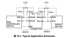
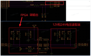
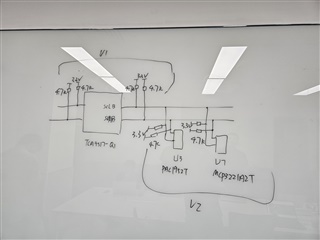
The schematic diagram of TCA9517-Q1 is shown in the following figure. Port A and port B use the same power supply, and the Pull-up resistor is 4.7k. The FPGA drives IIC. The output voltages of port A and port B pins SCL and SDA are both high. Six of 100 circuit boards have such problems. Please help review the schematic diagram and analyze the causes;
Based on the above issues, the customer has conducted the following tests, please refer to.
1. Replace with a new device, the IIC input and output levels are normal;
2. Make port A and port B power(3.3V) independent, the IIC input and output levels are normal;
3. Port B has three groups of Pull-up resistor. Remove any one or two groups, the IIC input and output levels are normal;
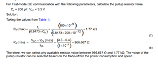
4. By changing the resistance value of port A or port B Pull-up resistor, for example, changing it to 11K,By changing the resistance value of port A or port B Pull-up resistor, for example, changing it to 11K,the IIC input and output levels are normal. Is there any suggestion or calculation formula for the selection of Pull-up resistor value?
Thanks!