This thread has been locked.

If you have a related question, please click the "Ask a related question" button in the top right corner. The newly created question will be automatically linked to this question.

THVD8000: Anti-interference design

Part Number: THVD8000

Hi team,

When we tested THVD8000, RS was very easy to be disturbed.
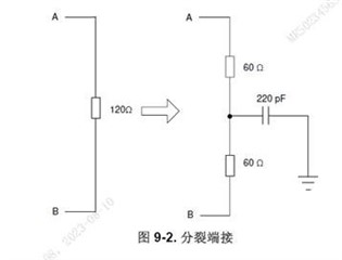
The current configuration is differential mode, the carrier rate is 2M, and the anti-common mode interference design is adopted. In the final test, the bit error rate of RS is 50%, and it is still 20% after adding the magnetic ring.


Questions:
1. What other methods are there to improve the anti-interference ability of this scheme?
2. This product is also used in electric power and building automation. How is the anti-interference design realized?

Thanks!

Rayna

  • Hi Rayna,

    1, So in addition to a split termination as you have shown above the next most common addition would be a common mode choke if interference is a big worry. Depending on system setup the use of filtering capacitors may also be used. In general we don't see them that much, but ferrite beads are also an option. 

    Above are the general components you can use to help mitigate emission issues. However, bit loss may not be 100% due to interference - as system layout is extremely important to proper communication.  So for you answer to question 2 please see below:

    2. Besides adding EMC friendly components the most important aspect of high SI THVD8000 is bus architecture + system layout.

    If you could provide a schematic with the following information it will help me check the bus architecture. 

    2a. How many nodes are in the system.

    2b. What is the data rate (I know the modulation is 2MHz - but what data rate are you trying to pass?)

    2c) How long is the bus

    2d) If there are more than 2 nodes in the system - what is the network topology (daisy chaining is by far the best - everything else will be worse for SI perspective) 

    2e) What Type of cabling are you using in the system? 

    2f) Is every communication node connected to a power load or power source node? 

    Please let me know on the questions for point 2 so I can better look into this system specifically. In general:

    1. Common mode Loading >= 375 Ohms at Modulation Frequency

    2. Series Capacitors <= 5 Ohms at Modulation Frequency

    3. If more than 2 nodes in system - they are daisy chained; unterminated stub lengths generally max out around ~300mm to 500mm with the THVD8000 so daisy chaining reduces stub length to a few mm preventing issues here. 

    4. Cable has 120 Ohm characteristic impedance. 

    5. Two nodes (terminal nodes) are terminated (split termination or standard) 

    6. Max Data Rate <= 1/10th of modulation frequency. 

    7. Unterminated Stub (for non-terminal nodes) are maxed out to 300mm to 500mm - or else you will get reflections.

    These is the most important aspects - so if you can share your schematic (even if its just of the 1 THVD8000 node (assuming the others are very similar)) it would be helpful to understand if all the basic guidelines have been followed to see what improvements need to be made - because if the above conditions aren't satisfied I don't think EMC friendly components will fix the issue. 

    Please let me know!

    Best,

    Parker Dodson 

  • Hi Parker,

     I attached the schematics and layout for your reference.

    customer feedback that the UART communication baud rate is 230400, the communication is 400 data packets per second, and each packet is 12 bytes. Setting the carrier frequency to 2MHz (5MHz anti-interference is the same as above), adding capacitors, ferrite beads, common mode inductors, three-terminal filter capacitors and magnetic rings before the A and B channels can't significantly robust EMC radiation anti-interference and conduction anti-interference.


    RS test conditions: 20V/m, 80MHz-1GHz.
    Communication packet loss is serious, under the interference of 80MHz-240MHz frequency band, or 270MHz-340MHz frequency band, more than 200 data packets are lost per second.
    Reduce the RS test condition to 12V/m, no effective improvement.

    CS test conditions: 0.15MHz-80MHz.
    The data packet loss is also serious, which can be effectively improved by adding multiple magnetic rings, and finally there is no packet loss.
    Bus length: 3.5 meters, the cable is an ordinary cable and cannot be shielded.
    There are two communication nodes in total, one end is connected to the host computer, and the other end is connected to the application part.

    Is there any more suggestion for improving the anti-interference performance?

    THVD8000 layout.docx

    Thanks!

    Rayna

  • Hi Rayna,

    A few comments on the schematic - as anti-interference also is going to require a larger SNR - which means you cannot overload the bus - this design is overloading the bus. 

    C19 and C20 alone violate common mode loading of THVD8000 - at 2MHz they are appx. 142 Ohms of impedance - the absolute minimum impedance of common mode loading allowed is 375 Ohms. By overloading the bus your signal strength is greatly reduced and any interference is going to have a lot more impact on the system.

    C13 and C14 are worse because they are at 1nF - so almost double C19 and C20. 

    Your inductors are too small - at 2MHz with 2 nodes that puts you at 60.2uH of effective inductance per node and this is assuming no filter caps - with filtering caps you will need more inductance - in general filter caps are the worst EMC elements you can add to Powerbus /RS-485 because of the common mode loading requirement - your customer has 10uH (L1 and L2) - this is also part of the common mode loading specification so the total common mode loading (inductors, filter caps, and other transceivers) on the line must maintain a common mode impedance of 375 Ohms or higher. At 10uH - assuming no derating from power supply current - you are at about 125 Ohms per inductor - so 1 inductor alone is already overloading the bus. 

    Next the DC source supplied through the inductors has no bulk capacitance - which is assumed to be there. I.e. the DC supply needs to have bulk capacitance or the coupling network will not work as described. At 2MHz - even something like a 100nF or 1uF should probably be more or less okay - but something needs to be there or else there can be interference issues. 

    I will say that the data rate they are using is higher than we suggest - at 2MHz we don't suggest above 200kbps - so there could be duty cycle distortion greater than +/-2%; however, it probably isn't that large of an issue with a shorter bus like this - but if they want to remove any risk they need to up the modulation frequency higher (at least 10x data rate).

    So just by the basic schematic alone - this design isn't going to most likely work - there needs to be some updates. 

    Next I do have a few comments on layout - but due to the difference needed in inductors most likely this is going to change. 

    The inductors are parallels and close to the bus - it would be more ideal to have the current in the inductor flow in the y-direction not the x-direction as it is right now. This is because the magnetic field runs perpendicular to the current flow - and in the current setup that means the inductor is better position to couple with the bus through its magnetic field. 

    There are two connections that may be better served with polygon pours instead of traces:

    On the termination portion is where my concern is:

    The items circled in blue should be changed into polygon pours. They are all connected to the same net - and this  layout is adding more corners to potentially cause issues with higher frequency energy as well as increasing the current density. This can be solved by just making these pours and not traces. 

    Another concern is the GND connection of the inductor / THVD8000

    There are only two vias on a pretty small trace - it may be a good idea to add another via and maybe widen the trace a little bit to prevent too much ground shifting. 

    Also there is unnecessary curves that exist on that trace that should be corrected. 

    I have added a design calculator in order to allow customer to quickly size components. Since the application is terminated ignore any box for unterminated systems (there are a small percentage of use cases where the system doesn't need to be terminated - this does not apply to this system).

    7853.THVD80x0_Design_Calculator.xlsx

    Please let me know if/when they can complete the new design. 

    Best,

    Parker Dodson