Hi Expert,
Do we know the substrate for the pin size(without ball)?
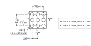
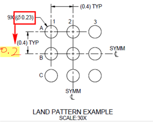
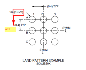
My customer can't do the via on pad(GND pin) on type 3 PCB, so they plan to reduce the footprint size for layout routing(0.23 to 0.22). Is there any side effect for reduce the ball?
Hi Expert,
Do we know the substrate for the pin size(without ball)?
My customer can't do the via on pad(GND pin) on type 3 PCB, so they plan to reduce the footprint size for layout routing(0.23 to 0.22). Is there any side effect for reduce the ball?