This thread has been locked.

If you have a related question, please click the "Ask a related question" button in the top right corner. The newly created question will be automatically linked to this question.

SN65DSI83: LVDS corrupted when using the DSI83 (follow up).

Part Number: SN65DSI83
Other Parts Discussed in Thread: DS90CF363B, SN65DSI86,

Hello everyone,


I opened this new thread to continue debugging the issues described on the ticket below.

https://e2e.ti.com/support/interface-group/interface/f/interface-forum/1231429/sn65dsi83-lvds-screen-corrupted-when-using-the-dsi83

As mentioned on my previous thread, we are facing some sporadic visual glitches when using the following setup: i.MX8MM + DSI83 + ds90cf363b + LCD, and on the previously mentioned ticket there were discussed some aspects regarding the DSI83 initialization sequence, and some DSI measurements.

Our bigger concern was that the DSI CLK signal amplitude was bigger than the expected, first it is 700mVPP and then it stabilizes to 400mVPP, we are reviewing with the NXP team why does the DSI signals have a bigger amplitude when being measured, I can confirm that we are measuring the clock using a differential probe on the CLK_P and CLK_N signals. But I would like to ask you some additional questions, please find them listed below.


1.- As per our latest measurements there seems that the DSI clock has a much bigger amplitude (~700mV pp) when the DSI83 EN signal is asserted low, based on your experience with the DSI83 is this a normal behavior?


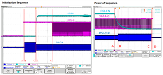
2.- At this point assuming that the DSI CLK amplitude was correct, the initialization sequence would match the requirements, as our customer device is an Android based tablet, where the screen can be locked and unlocked several times, does the previously illustrated power off sequence is correct? As far as I saw the DSI CLK, and data lanes are in HS when DSI83 EN ramps from high to low.


3.- In the past I worked with the SN65DSI86 DSI to DP bridge, which supported a reduced range of resolutions when the DP PLL was being obtained from the DSI clock and did not have this limitation when using an external oscillator as reference clock.

On our SN65DSI83 DSI to LVDS bridge, the LVDS pixel clock is derived from MIPI D-PHY CLK, does the DSI83 have a similar limitation with the supported resolutions? Our goal is to work with the following video timings using 2-DSI lanes.


Any guidance will be highly appreciated,

Thanks, and best regards,

Esteban V.

  • Hey Esteban,

    Regarding your questions:

    1) The change in the voltage swing has to do with the terminations changing when the DSI clock switches in and out of HS mode. This is normal behavior.

    2) The power down sequence looks ok, but I would say that passing data after the DSI-EN is pulled down is unnecessary. Please refer to Section 8.1.1 in the Sn65DSI83 datasheet for the proper video stop sequence.

    3) The DSI83 should not have this limitation, but an external oscillator will have less jitter and be a cleaner clock. 

    The display spec clock lines up with the LVDS output clock spec, so the SN65DSI83 should work with your application.

  • Hello Vishesh Pithadiya,


    Thank you very much for your quick response, please find my comments below.

    1.- Understood, thank you for the clarification.

    2.- Ok, we will implement a power down sequence which matches the datasheet specification.

    3.- Ok, regarding this item, the issue is very sporadic (occurs 1 of 100 times when locking and unlocking the device screen) and it is random (sometimes it occurs almost immediately and other times it takes a long time to be reproduced), and the initialization sequence is the same when the image is correctly displayed and when it is corrupted, I am wondering if the external reference clock could help removing the issue, on your experience could this be the case?

    4.- When measuring the DSI CLK, when the clock stabilizes after DSI83 is asserted, the signal amplitude is around 400mVPP approximately, on my previous ticket we were told that this amplitude was not the expected one, but just to double check, could this be an issue that causes the observed glitch?


    Looking forward to your comments,

    Thanks, and best regards,

    Esteban V.

  • Hey Esteban,

    In general the sporadic issue can be caused by excessive jitter at the clock, so switching to an external clock may solve the issue. However, I cannot say for 100% what the issue is or how to solve it without more information.

    My suggestion is to try implementing an external clock in your test setup if possible, and try to replicate the issue you were having before. 

    Another thing I noticed is that the clock frequency needed for your panel is 25MHz, and the LVDS output frequency range is 25MHz to 154MHz. There may be an issue with the panel being in the edge range for the SN65DSI83. 

    You could try using another display if possible and see if the issue persists there as well.

    Let me know if either suggestion fixes the issue?

  • Hello Vishesh Pithadiya,


    Thank you for the quick response, understood I will check with the team to see if the PCB can be reworked for it to use an external oscillator as a reference clock.

    According to our LCD timings, does 25 MHz would be the correct external oscillator frequency? And from the code perspective there would only be needed to modify the 0x0A (HS_CLK_SRC) and the 0x0B (REFCLK_MULTIPLIER) I2C registers is my understanding correct?

    We cannot test a different LCD; however, we have tried to set the pixel clock at 25MHz and 27MHz since both are supported by the panel, but the issue occurrence is the same when working at these frequencies, was this issue observed before on similar panels?

    It is important to say that if the issue occurs and we send the DSI83 test pattern using the 0x3C register, the pattern is displayed correctly, but when returning to normal operation the issue is there again, the issue can be temporarily fixed by locking and unlocking the tablet screen, which reinitializes all the video core of the device.


    Looking forward to your comments,

    Thanks, and best regards,

    Esteban V.

  • Hey Esteban,

    If the test pattern is displaying correctly and doesn't have the issue, but the issue persists when you're sending a DSI signal to the panel then this issue is on the DSI side rather than the LVDS side of the SN65DSI83. 

    Could you take a look at all the values of the DSI registers you are using? All of them are explained  in table 7.6 of the SN65DSI83 datasheet. Based off of the info you have provided I believe that the issue is coming from an incorrectly set DSI register. If there is any confusion regarding how to generate the proper register values don't hesitate to ask.

    If you have any more questions please let me know!

    Best,

    Vishesh Pithadiya

  • Hello Vishesh Pithadiya,


    Thank you for your quick response, please find my comments below.


    1.- Our customer agreed to test an external reference clock by reworking a PCB even if this is only a hypothesis, for us to isolate the root cause of the issue, so, could you please let me know which would be the frequency of an external oscillator to be placed on our PCB according to the LVDS panel timings? In a similar fashion could you confirm that on this case the only registers to be modified on the code are the 0x0A (HS_CLK_SRC) and the 0x0B (REFCLK_MULTIPLIER)?

    2.- Regarding the DSI register configuration (table 7-6) I have some questions, regarding the CHA_DSI_LANES our hardware has 3 DSI lanes connected between the i.MX8MM and the SN65DSI83, but as per some known issues with the i.MX8MM DSI host controller we are only configuring through software 2 DSI lanes to be used, the SN65DSI83 datasheet stages that: “Unused DSI input pins on the SN65DSI83 must be left unconnected” having three DSI lanes connected but only working with two could be an issue?

    3.- In a similar fashion to questions #2 according to our LVDS panel timings, working with two DSI lanes would be correct?

    4.- Our driver does not configure any of the following register fields: SOT_ERR_TOL_DIS, CHA_DSI_DATA_EQ, and CHA_DSI_CLK_EQ could this be an issue?

    5.- Regarding the CHA_DSI_CLK_RANGE our driver configures the 0x1E value, our DSI clock is 150MHz and it is given by the following equation.

    (Pixel clock * bits per pixel) / (2 * DSI lanes) =

    (25MHz * 24) / (2 * 2) = 150MHz

    As per my understanding this register has been correctly set, but could you please double check?


    Any guidance will be highly appreciated,

    Thanks, and best regards,

    Esteban V.

  • 1) the frequency at the output for the LVDS signal will be the same as the panel spec. 25 MHz should be the correct frequency for REFCLK. The registers that need to be modified are 0x0A and 0x0B. No multiplier will be needed if you use a 25 MHz clock, but you can multiply up if a slower clock is used. 

    2) The unused channels that are connected could be an issue as there is a higher probability of crosstalk. The best option is to remove the issue entirely by disconnecting all lines not in use and terminating them based on the datasheet. 

    3) Two DSI lanes should be fine, but double check the timings on the inputs and outputs following this FAQ: https://e2e.ti.com/support/interface-group/interface/f/interface-forum/852871/faq-sn65dsi84-no-display-output-with-sn65dsi83-sn65dsi84-sn65dsi85

    4) These register fields should play a role, unless there are heavy channel losses from the source to the DSI inputs. To see if using these are necessary check the loss of the cable/ trace that is connecting the DSI signal source to the SN65DSI83 DSI input. 

    5) The 0x1E value should be correct, but try 0x1D and see if that fixes the issue. 

    Let me know if you have any more questions.

  • Hello Vishesh Pithadiya,


    Thank you for your quick response, please find my comments below.

    1.- Understood, so we will proceed testing a 25MHz reference clock, so on the code there will only be needed to set the 0x0A register BIT#0 to 0 (LVDS pixel clock derived from input REFCLK), then 0x0B register BITS#7:3 (DSI_CLK_DIVIDER) must be set to 00000 and BITS#1:0 (REFCLK_MULTIPLIER) must be set 00 since a 25MHz clock will be used, is my understanding correct?

    2.- Thank you for the confirmation regarding the 2 DSI lanes, I will check with our team if we can rework the board for the unused lanes to be properly disconnected.

    3.- Understood thank you for the clarification.

    4.- How could I determine if there is needed to set any of these bits? Could you please explain it to me a bit more?

    5.- I agree with you that 0x1d could be a valid value since it is on the following range: 145<=freq<150, however today I tested it and the issue still occurs.


    At this point based on what we have discussed, I think that the best path forward, would be first modifying the IC power down sequence according to the 8.1.1 section of the SN65DSI83 datasheet then if it does not works, try disconnecting the unused DSI lanes, and finally if the issue persist take the approach of using a 25MHz external oscillator as a reference clock, do you have any additional recommendation/consideration for us to debug this issue?


    Looking forward to your comments,

    Thanks, and best regards,

    Esteban V.

  • 1) yes the DSI_CLK_DIVIDER would be set to all 0s, and the REFCLK_MULTIPLIER would also be set to 0s as there is no multiplication of frequency. 

    4) You would need to look at the insertion loss of cables. Basically send a signal from one end of the cable/trace and measure it at the opposite end. Using the measured signal and the original sent signal determine how many dB of loss the cable/trace has. If this loss is a high value we can use the equalization registers to offset that loss with a gain. 

    Based off of the data provide this looks like a good way to progress forward and debug this issue!

    Best of luck :)

  • Hello Vishesh Pithadiya,


    Thank you for your comments, and sorry for my late response, we have received some feedback from the hardware team, please find their comments below.


    1.- Regarding letting unconnected the unused DSI pins, we disconnected the data lane #2 (P/N), however the issue still occurred with this rework, does there is needed any specific consideration for the pins to be correctly disconnected?

    2.- Regarding the external oscillator, we reworked a device, but the sporadic issue still occurred, additionally image on screen is a little bit corrupted every time, and the original issue can also be seen, I asked for more information about how the rework was done, for us to share it with you.

    3.- Regarding the STOP/restart sequence described on section 8.1.1, I saw that there is mentioned that DSI lanes must remain on LP11 but CLK lanes in HS, it is important to say that when stopping the video stream our SoC sets the data and clock lanes on LP11, could this be an issue?


    Looking forward to your comments,

    Thanks, and best regards,

    Esteban V.

  • Hey Esteban,

    Leaving them disconnected should be fine. try pulling them to ground and see if that helps, but they should be good as they are.

    Implementing an external oscillator should clean up the video and clock, so there must be either a slight mismatch in frequency or some other issue in the rework. Make sure the differential resistances at the output LVDS signals are all matched as well. should be around 180 ohms. 

    I will look into the STOP/restart sequence and get back to you by EOD today.

  • Hey Esteban,

    Upon further inspection of the STOP sequence it is most likely an issue that the CLK is driven to the LP11 state, try changing up the procedure to leave the CLK in the HS state when powering down.