Hi,
we want to use the DP83TC813 PHY in our product. So, there is prototype board with the chip.
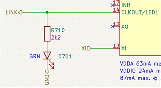
When testing the chip we had some problems with CLKOUT/LED1 GPIO. We are not able to configure it with SW to be LED1 and not CLKOUT. Currently the chip always generates 25MHZ clock out of the pins, even if we configure it via MDIO interface as LED1.
We tried following:
Configure Pin 14 (CLKOUT/LED1) to a link status LED:
1. Set Register LEDS_CFG_1 (0x450) to 0x0000 (normal operation, 20 Hz blink rate, LED0/1/2 Link OK)
2. Set Register LEDS_CFG_2 (0x451) to 0x0000 (all CLKOUT MSB 0, normal drive operation, active low)
3. Set Register IO_MUX_CFG_1 (0x452) to 0x0000 (clk src = don't care, LED_1 = LED_1, LED_0 = LED_0)
4. Set Regsiter IO_MUX_CFG_2 (0x453) to 0x0000 (led1 is led1, clk src don't care, clkout is LED_1)
Now LED_+/CLKOUT should be a link status LED output. But I get a 25 MHz clock.
When reading out IO_STATE_1 (0x457) a random value in the CLKOUT bit is set, so the pin seems to be treated as an input.
Additionally, I tried various configuration, e.g. a different clk source, clk divider and some invalid ones) for the clk output and the non-existing LED_0 and LED_2 pins but nothing changed the 25 MHz clk output on LED_1.
Could someone support me with the topic. Many thanks.
Best,
Mykola

-
Ask a related question
What is a related question?A related question is a question created from another question. When the related question is created, it will be automatically linked to the original question.