This thread has been locked.

If you have a related question, please click the "Ask a related question" button in the top right corner. The newly created question will be automatically linked to this question.

SN65LBC174A-EP: part details

Part Number: SN65LBC174A-EP
Other Parts Discussed in Thread: SN65LBC173A-EP, SN74LVC1G17-EP

Need following clarifications:

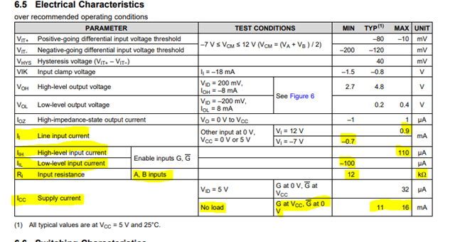
  1. What is the input/output capacitances and Impedance for input pins for IC: SN65LBC174A-EP?
  2. Do you have reference for power loss calculation for IC: SN65LBC174A-EP if using 1 channel of the IC?
  3. What is the input/output capacitances and Impedance for input pins for IC: SN65LBC173A-EP?
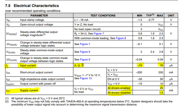
  4. Do you have reference for power loss calculation for IC: SN65LBC173A-EP if using 3 channel of the IC?
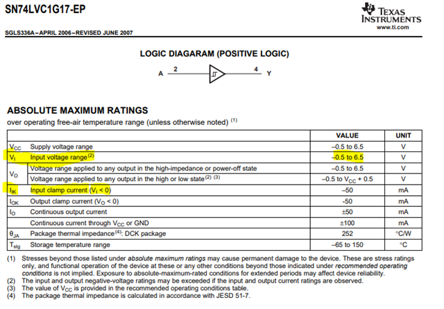
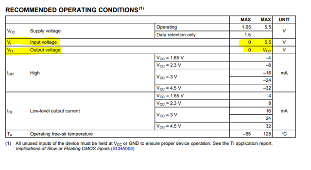
  5. For buffer IC: SN74LVC1G17-EP, if supply voltage Vcc is 3.3V will there be an issue if 5V signal is given as input at pin A?
  • E2E Team, 

    Please provide your inputs on high priority.

    Regards,

    Dnyanesh

  • Hi Prahlad,

    So we don't really specify a lot of these characteristics directly for the SN65LBC17xA-EP devices - what we have in the datasheet is pretty much it. 

    For Questions 1 and 2:

    We don't specify capacitance as it generally, in vast majority of cases, doesn't matter in these applications because the capacitive loading of the driver is generally >> than any capacitance the device has. 

    Input Impedances can be roughly approximated from the input current spec - at worst case you see 70uA which would happen at VCC = 5.25V - which would give an input impedance of about 75K - generally it will most likely be higher in most applications as this is worst case approximation. 

    For power consumption - its very dependent on loading - you can make a rough approximation from the ICC supply current that each driver takes appx. 375uA when disabled and 6.25mA when enabled - however at least 2 driver will always be active with the 174 - you cannot have 1 driver only. This specification also only includes Idle current - so your power consumption really is determined by the loading - we do have a generalized paper to help with power calculations - but the main take-away is that you just need to sum the power consumed at each pin - which is extremely dependent on system setup and loading. So we won't be able to give you a solid estimate because of the variability in teh system setup - we can give you the idle current. 

     https://www.ti.com/lit/an/snoa233b/snoa233b.pdf?ts=1698681450094&ref_url=https%253A%252F%252Fwww.ti.com%252Fsitesearch%252Fen-us%252Fdocs%252Funiversalsearch.tsp%253FlangPref%253Den-US%2526searchTerm%253Drs-485%2Bpower%2Bdissipation%2526nr%253D30 

    For questions 3/4

    Same issue with capacitance - it is not specified on this device; most of our RS-485/RS-422 devices do not have this specified, although on newer devices it is more commonly specified. 

    For input impedances:

    on the A/B pins - Ii and Ri both can tell you input impedance. 12K is the most common value most designers would use here. 

    For the enable pins it depends if it is a low or a high - but should be between 45K and 50K approximately worst case. 

    For power - all channels will be active or disabled -you can't have any other configuration - so the power we spec in the datasheet is the idle power you can expect. This power consumption will most likely increase based on system setup and the loading on the output pins of the 173A. 

    5. 

    The voltage input range on the SN74LVC1G17-EP is -0.5v to 6.5V - it is not dependent on VCC - this is further shown as the input clamp only conducts on negative inputs - so there is no diode from A to VCC - so applying 5V to A when the device is at VCC = 3.3V will not harm the device. It is also shown in the recommended operation conditions that in the input voltage is suggested to be 0V to 5.5V - not dependent on VCC - whereas the output voltage max is VCC. 

    Best,

    Parker Dodson