Hi team,
I have a customer with the below list of questions. I'd greatly appreciate your assistance with this!
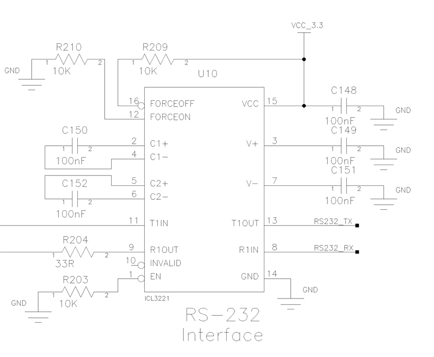
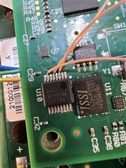
"We use the above RS232 transceiver on at least one of our designs. I was recently asked to look in to an issue that our CM is having at ICT. I’m pretty sure that it’s a problem with their test but they claim the test was passing on older devices and has started failing with newer devices. The test they are performing involves measuring the voltage at the C2+ pin. I believe they are looking for 3V DC but I’m not sure how they arrived at this. Since this pin is part of the charge pump circuit, I question the validity of the test but as I said, they have been doing this successfully for some time and have recently started seeing issues. I’m still in the process of getting more information from the CM but I have a few questions about the device.
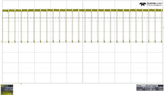
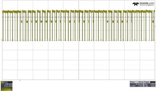
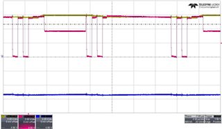
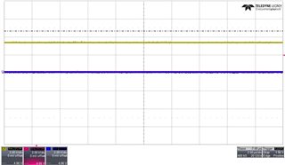
- Since C2+ is a node in the charge pump circuit, I assume it is a switching node and not DC. Is this correct? Can you give me an idea of what the waveform at this pin might looks like?
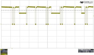
- Is the C2+ a high impedance input? When I probe the pin with a 10M passive probe that is grounded, I get the device to fail? When the gnd on the probe is not connected, the device continues to work.
- PCN 20210720000.1 was issued several years ago. Any idea if the charge pump circuit changed in some way that might explain why the test passed on older devices and no longer passes?"
Thanks in advance
Marco