This thread has been locked.

If you have a related question, please click the "Ask a related question" button in the top right corner. The newly created question will be automatically linked to this question.

TCAN4550-Q1: Trouble with TCAN4550-Q1 CAN Controller

Part Number: TCAN4550-Q1
Other Parts Discussed in Thread: TCAN4550

Hello, 

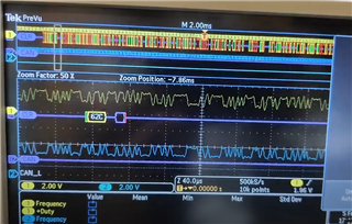
I'm currently working on configuring the CAN bus using the TCAN4550-Q1 CAN controller with SPI interface on an Ambarella platform. While I've been able to establish the can0 network interface and confirm loopback functionality using canutilitis, I'm encountering issues when attempting to trace messages using tools like CANoe or PCAN.  I can observe waveform data on the CAN wires using an MSO 

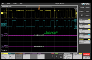
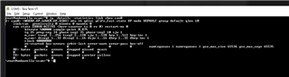
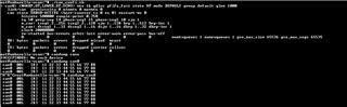
root@-:~# ip -details link show can0
2: can0: <NOARP,UP,LOWER_UP,ECHO> mtu 16 qdisc pfifo_fast state UP mode DEFAULT group default qlen 10
    link/can  promiscuity 0 minmtu 0 maxmtu 0
    can state ERROR-ACTIVE (berr-counter tx 0 rx 0) restart-ms 0
          bitrate 800000 sample-point 0.800
          tq 25 prop-seg 19 phase-seg1 20 phase-seg2 10 sjw 1
          m_can: tseg1 2..256 tseg2 2..128 sjw 1..128 brp 1..512 brp-inc 1
          m_can: dtseg1 1..32 dtseg2 1..16 dsjw 1..16 dbrp 1..32 dbrp-inc 1
          clock 40000000 numtxqueues 1 numrxqueues 1 gso_max_size 65536 gso_max_segs 65535

  • Hi Anand,

    If you are seeing signals on the CANH and CANL pins that when the TCAN4550 transmits a message, then perhaps there is an issue with the bit timing configuration matching those of the CANoe and PCAN.  What do the waveforms for a full CAN message frame look like?  Are the messages getting acknowledged, or are there error flags being generated by the CANoe and PCAN modules?  Can you capture and provide the waveforms for a full CAN message?

    Can you confirm what the Nominal and Data bit timing settings are for both the TCAN4550 and CANoe and PCAN modules?

    Regards,

    Jonathan

  • Hi Jonathan, 

     Thanks for your reply, I've tried matching the sample-points, phase segs values of the target to the deafault values of PCAN tool, And I was gettting BUS HEAVY and then BUSOFF error on the trace window while I sent messeges from the target device and sometimes messeges are not being acknowledged, Scope also is reading Error Frames/ unexpected Data on the lines, Also I've measured the resistance accross the test points of the CANH and CANL wires and I'm getting value 124 Ohms, could this be also one of the reason, I've attached the images below.

  • Hi Anand,

    I don't have direct experience with the PCAN analyzer tool you are using, but through some research I have found that other's have said the BUS HEAVY fault is either due to incorrect or missing bus termination, or incorrect bit timing settings, and the clock source may not be adequate and they referenced an 8MHz clock frequency.

    A properly terminated CAN bus has two sets of 120 ohm termination resistors with one set placed at each end of the bus.  They are in parallel so the bus impedance should be approximately 60 ohms.  Because you are measuring 124 ohms, I suspect you are missing a set of termination resistors which could be leading to the errors.

    I also see in your screenshot of the PCAN configuration that it shows a clock frequency of 8Mhz.  Typical clock frequencies used in CAN are higher such as 20MHz, 40MHz, 80MHz, etc.  Do you have a faster clock option?

    If you can provide me a schematic diagram of your setup and TCAN4550 circuit, I can review that for any possible errors or improvements.

    If you can provide me a list of the final register values you are using in your TCAN4550 configuration, I can also review that for any possible issues.

    Regards,

    Jonathan

  • Hi Jonathan,

    The TCAN4x5x driver code used in our project is sourced directly from the official Linux kernel repository hosted on GitHub at [https://github.com/torvalds/linux/tree/master/drivers/net/can/m_can. I have not made any modifications to the driver code itself. As per my understanding the specific register values are typically determined by the initialization routines, interrupt handlers, and configuration settings applied during runtime Slight smile,

    I have attached a schematic diagram illustrating the setup of the TCAN4550 circuit within my system.

    Thank you for your support.

    Regards,

    Anand Kulkarni

  • Hi Anand,

    I understand you are using the Linux community's driver code and that it will set many of the configuration registers during runtime.  This unfortunately doesn't not provide me with any information to help you debug your issues because I don't know how the device is configured, and I don't know what status and interrupt bits may be getting set that could indicate the issue.

    I believe there are functions in the driver for reading the TCAN4550 registers.  Is it not possible to simply read back all of the device register to some form or log file or to a UART terminal at the end of the configuration sequence so that we can verify what settings the driver code is using and make sure the bit timing settings match the PCAN settings?

    I see one issue with the schematic but I'm not sure it is causing any troubles at this time.  The series resistor between the OSC2 pin and the crystal (R384) should be located between the OSC1 pin and the crystal.  The OSC1 pin is the "output" of TCAN4550's current transconductance amplifier feeding current to the crystal, and the OSC2 pin is the "input".  This is common misunderstanding because when a single-ended clock is used instead of a crystal, the OSC1 pin becomes the "input" pin for the single-ended clock and the OSC2 pin is grounded.

    You can reference the TCAN455x Clock Optimization and Design Guidelines application note for more information. (Link)

    Regards,

    Jonathan

  • Hello Jonathan,
      As I am relatively new to this task, I'm uncertain if this approach is correct, I have attempted to read the register values through SPI using the following code :

    Fullscreen
    1
    2
    3
    4
    5
    6
    7
    8
    9
    10
    11
    12
    13
    14
    15
    16
    17
    18
    19
    20
    21
    #include <stdio.h>
    #include <stdint.h>
    #include <unistd.h>
    #include <fcntl.h>
    #include <sys/ioctl.h>
    #include <linux/spi/spidev.h>
    static const char *device = "/dev/spidev2.0";
    static uint8_t mode = SPI_MODE_0;
    static uint8_t bits = 8;
    static uint32_t speed = 1000000; // 1 MHz
    static uint16_t delay = 0;
    #define REG_MCAN_CREL 0x1000
    #define REG_MCAN_ENDN 0x1004
    #define REG_MCAN_CUST 0x1008
    #define REG_MCAN_DBTP 0x100C
    #define REG_MCAN_TEST 0x1010
    #define REG_MCAN_RWD 0x1014
    #define REG_MCAN_CCCR 0x1018
    #define REG_MCAN_NBTP 0x101C
    XXXXXXXXXXXXXXXXXXXXXXXXXXXXXXXXXXXXXXXXXXXXXXXXXX

    Below are the outputs I obtained before and after setting up the CAN network interface:

    Fullscreen
    1
    2
    3
    4
    5
    6
    7
    8
    9
    10
    11
    12
    13
    14
    15
    16
    17
    18
    19
    20
    21
    [14:55] Anand S. Kulkarni
    root@ambarella-vcam:/usr/bin# testtcan
    Value from REG_MCAN_CCCR register (little-endian): 000C4800
    Value from REG_MCAN_CREL register (little-endian): 00004866
    Value from REG_MCAN_ENDN register (little-endian): 00024866
    Value from REG_MCAN_CUST register (little-endian): 00044866
    Value from REG_MCAN_DBTP register (little-endian): 00064866
    Value from REG_MCAN_TEST register (little-endian): 00084866
    Value from REG_MCAN_RWD register (little-endian): 000A4866
    Value from REG_MCAN_NBTP register (little-endian): 000E4866
    Value from REG_MCAN_TSCC register (little-endian): 00104866
    XXXXXXXXXXXXXXXXXXXXXXXXXXXXXXXXXXXXXXXXXXXXXXXXXX

    your guidance on whether this method provides accurate insights into the device's configuration would be immensely helpful.

    Regarding the series resistor in the schematic (R384), I can confirm that it is indeed 0 ohms. Despite its value, could its placement between the OSC2 pin and the crystal still potentially affect the stability of the oscillator circuit and introduce impedance mismatch?

    Thank you once again for your assistance and valuable expertise.

    Regards,

  • Hi Anand,

    Thanks for the register information, however, I'm not sure they are correct just by looking at the values.  It appears the lower two bytes are always either 0x4866 or 0x6666 which would not be normal.  I've looked through a few of the registers such as the Nominal Bit Timing and Prescaler  (NBTP) and the timing does not work for a 500kb bit rate.

    Can you try to verify these registers are being read back correctly?  The Device ID registers 0x0000 and 0x0004 should always return a known value.  Also the Test and Scratch Pad register 0x0808 can be used to write a value and then read it back to verify both the Read and Write SPI communication is working correctly.

    Thanks and Regards,

    Jonathan

  • Hi Jonathan,

    I apologize for the delay in reaching out to you. I've been troubleshooting an issue,I have made progress in receiving CAN messages successfully from both PCAN and CanOe,  
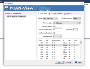
I am encountering challenges with transmitting messages from the target device. TCAN4x5x controller is successfully receiving data from both PCAN and CanOe.

    However, when attempting to send messages from the target device, the external receiver detects the message only once. Upon inspection, the received messages appear to lack any data payload.

    I have attempted to read and write to the registers using the functions provided in the driver code. However, despite successfully writing to the Test register, the value read from the register remains at 0.

    Fullscreen
    1
    2
    3
    4
    5
    6
    7
    8
    9
    10
    11
    12
    [ 3.064191] tcan4x5x spi3.0: no CAN clock source defined
    [ 3.070293] tcan4x5x spi3.0: setup mode 0, 8 bits/w, 10000000 Hz max --> 0
    [ 3.088392] TCAN4x5x Device ID0: 0x32150320
    [ 3.092575] TCAN4x5x Device ID1: 0x87654321
    [ 3.098278] TCAN4x5x Revision: 0x0
    [ 3.102649] TCAN4x5x Status: 0xa33
    [ 3.106285] TCAN4x5x Error Status: 0x80
    [ 3.110203] TCAN4x5x Interrupt Flags: 0x80
    [ 3.110766] iio iio:device1: registered accelerometer lis2dw12
    [ 3.114373] TCAN4x5x Control: 0x0
    [ 3.123524] TCAN4x5x MCAN Configuration: 0x0
    [ 3.127801] Value read from TCAN4X5X_TEST_REG: 0
    XXXXXXXXXXXXXXXXXXXXXXXXXXXXXXXXXXXXXXXXXXXXXXXXXX

    I look forward to your response.

    Thanks & regards,

    Anand 

  • Hi Anand,

    I have attempted to read and write to the registers using the functions provided in the driver code. However, despite successfully writing to the Test register, the value read from the register remains at 0.

    Are you referring to the "Test" register with address 0x1010?  If so, this is a read only register.  Or are you referring to the "Test Register and Scratch Pad" register with address 0x0808 that does support both Read/Write access?

    However, when attempting to send messages from the target device, the external receiver detects the message only once. Upon inspection, the received messages appear to lack any data payload.

    If I understand you correctly, the receiving devices (PCAN or CANoe) do see a message on the bus that is transmitted from the TCAN4550.  Does this message have the correct message ID and header bits based on what you are trying to transmit?  What is the DLC value in the message header?

    I have seen one previous situation that sounds similar to yours where messages were not containing any message data.  It turned out that the SPI communication was using multi-word writes when placing the message data into the TX Buffer element in the TCAN4550's MRAM.  However, the SPI chip select signal was transitioning high in between every 32-bit data word which was causing the SPI multi-word write to fail.  Only the first 32-bit word in the transaction that contained the message ID was getting placed into the TX Buffer.

    Do you have the ability to monitor the SPI signals with a logic analyzer?

    Can you read back the memory contents of the TX buffer that is being used to transmit the message?  If so, can you read it back and verify it matches the contents of your message including the correct DLC and data bytes?

    You can find the MRAM TX Buffer Element definition in section 2.4.3 of the M_CAN User's Manual published by Bosch (Link).

    Regards,

    Jonathan

  • Hi Jonathan,

    Thank you for your detailed response and suggestions, To clarify, I have been referring to the "Test Register and Scratch Pad" register with address 0x0808, not the "Test" register at address 0x1010. 

    Regarding the reception of messages from the TCAN4550, received messages lack any data payload, and the message ID does not match the expected values. The DLC value in the message header is also not as expected. Image below shows the receiver trace window.

    I am currently working on monitoring the SPI signals between data transfers using a logic analyzer to identify any anomalies.

    Additionally, I attempted to read the memory contents of the TX buffer being used to transmit the message. However, the data I retrieved from the M_CAN TX buffer did not match the expected contents of the message.

    I was sending messege with ID 123, data 12345678, and this is what I was getting from the FIFO
    [ 145.924597] Transmit FIFO Data[0]: 00000000

    I would greatly appreciate any additional suggestions or insights you may have, Looking forward to your response.

    regards,

    Anand Kulkarni

  • Hi Jonathan,

    I also want to mention one observation here, In our system, we utilize an external crystal with a frequency of 20 MHz. To accommodate this, I made the necessary adjustments by changing the clock definition in the tcan4x5x-core.c file from 40 MHz to 20 MHz. Consequently, this alteration enabled successful message reception within our system.However, upon conducting loopback testing, I noticed a same discrepancy in the results. Specifically, when performing loopback testing with the 20 MHz clock configuration, the received message appeared same as it is showing on the PCAN view trace : can0 000 [0] 

    This outcome contrasts with the expected behavior observed when the clock was defined at 40 MHz. Under the previous configuration, loopback testing yielded the anticipated results.

    But with 40 Mhz clock defined, when attempting to send messages externally and then receive them, it displays bus-off followed by bus-heavy conditions on the PCAN and CanOe.

  • Hi Anand,

    If you are unable to write and read back a value from the Scratchpad register 0x0808, and all your other read backs are returning "0's" when you try to read back the TX Message data, then I'm not sure whether it is just an issue with a write, read, or both functions.  It seems like there may be some issue with your SPI communication. 

    It appears like something is working because it you are seeing some device activity, but the odd behavior could be from some sort of SPI errors.  It would be good to verify the SPI signals with a logic analyzer or scope plot to see if there are any errors with them. A clock problem could also cause SPI communication errors. 

    If you notice, there are 3 different groupings of registers with different address ranges.

    The registers in the group with address 0x0000 to 0x002F are implemented in logic and only require the SPI clock.  They do not require the system clock supplied through the OSC1/2 pins to be active or working properly to interact with.

    The registers in the group with address 0x0800 to 0x08FF are device related registers not associated with the MCAN controller.  They do require the system clock to be functional so that the digital core can act upon the register read/write request coming in from the SPI bus.

    The registers in the group with address 0x1000 to 0x10FF are MCAN related registers are part of the Bosch MCAN IP.  These registers also require the system clock to be functional in order to access the registers as well as to send or receive CAN messages.

    There is a FIFO that handles the SPI clock domain to System clock domain translation on the SPI read/write data.  If the system clock has an issue, then there will be an error getting data through the FIFO and this will be reported in the Status register 0x000C that only operates off of the SPI clock domain.

    Can you read the registers 0x0000 to 0x0010?  Can you also try to write to register 0x0010 and read back the value you just wrote?  At the same time can you try to do the write/read test on the scratchpad register 0x0808 again to see if it still has an issue?  If the Sratchpad register doesn't work, but the other registers work then we may be able to conclude this is a clock issue.  If you also have issues with the registers 0x0000 to 0x0010 then there may be a protocol issue with your SPI signals.

    For the CAN message reception, I am confused a little and I'm not sure I understand.  In your first post today you mentioned that your received messages lacked any data payload and had an incorrect message ID.  But in your second post, you said that you made alterations to the clock configuration and this enabled successful message reception within our system.  Does that mean that the received messages contained the correct data payload and message ID after the clock configuration adjustment?

    What adjustments did you make?  Can you try again to get me a list of register values for the device?  The last time it appeared the registers had an incorrect value so I'm still not quite sure about the configuration you are using.

    Do you have the ability to capture the CAN messages on a scope for both the messages transmitted from the TCAN4550 and to the TCAN4550 from PCAN or CANoe?

    Regards,

    Jonathan