A related question is a question created from another question. When the related question is created, it will be automatically linked to the original question.
If you have a related question, please click the "Ask a related question" button in the top right corner. The newly created question will be automatically linked to this question.
Who is the OEM/ODM for this project, and what is the project name?
current setup is in pin-strap mode but no DDC snooping, could be a problem. Make sure CMC is within bandwidth of the HDMI signal used Make sure clamping voltage for ESD is ~5V
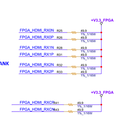
Why are the differential signals being pulled up to 3.3V?
Who is the OEM/ODM for this project, and what is the project name?-->ODM --> VEGA-3006
current setup is in pin-strap mode but no DDC snooping, could be a problem. Make sure CMC is within bandwidth of the HDMI signal used-->
Please explain again, I don't understand what you mean.
We currently have other projects to set PIN Strap. From FPGA Team feedback is have DDC Snooping. At the same time in the 4K source, it is verified PASS !
Make sure clamping voltage for ESD is ~5V-->
Please explain the component number ?
Why are the differential signals being pulled up to 3.3V?
-->Because the TMDS181 output is connected to FPGA, FPGA does not have the internal Pull Hi 3.3V Pin Type.Need external Pull Hi Please refer to TMDS181 DS Page15
We currently have other projects to set PIN Strap. From FPGA Team feedback is have DDC Snooping. At the same time in the 4K source, it is verified PASS !
Just wanted to make sure snooping was being done as I cant see the DDC connection to the FPGA.
Make sure CMC is within bandwidth of the HDMI signal used-->
I cant see the part number for the common mode choke(CMC) you are using, so I want to make sure that the CMC is good enough for HDMI 2.0 bandwidth. Here is a chart with many CMCs that should work for your application:
-->Because the TMDS181 output is connected to FPGA, FPGA does not have the internal Pull Hi 3.3V Pin Type.Need external Pull Hi Please refer to TMDS181 DS Page15
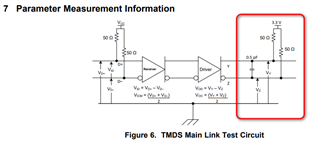
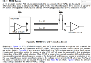
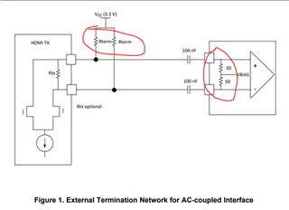
This circuitry was for parameter measurement, not for application use. This is the schematic for an AC coupled application. In practice they should be the same, but just for future reference.
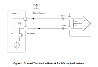
AC coupled implementation:
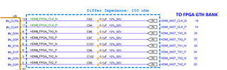
I didn't see the AC coupling circuitry at the bottom on the schematic, apologies. However, it seems there is a naming mismatch for the HDMI TX1 Clock.
The circuitry for U6 looks like its the same as U3, so all of the above should apply to U6 as well. Working on the U9 schematic review.
Here are some additional points I missed in my first run over the schematic review.
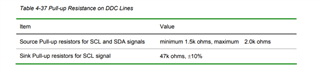
On the TMDS181, 40.2k pullup on DDC_SDA/SCL is out of HDMI spec, need use 47k +/-10%
For pin-strap mode, set TMDS181 TEST/A1 to NC
Set TMDS181 EQ_SEL to NC
For both DP159 and TMDS181, too many 4.7uF, keep one and replace rest with 0.1uF
FPGA input requires to be AC coupled, but TMDS181 output needs to be 3.3V common mode voltage, so use external 50ohm termination to 3.3V to set the CM. But 50ohm termination and FGPA input termination create double termination so output signal amplitude gets cut in offer. May need to adjust TMDS181 output SWING to compensate
Just wanted to make sure snooping was being done as I cant see the DDC connection to the FPGA.
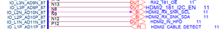
-->please view RX1 U4 & RX2 U7 & TX U10 is from DDC connection to the FPGA. I have confirmed from FPGA.
2.I cant see the part number for the common mode choke(CMC) you are using, so I want to make sure that the CMC is good enough for HDMI 2.0 bandwidth. Here is a chart with many CMCs that should work for your application:
--->Our Si simulation team recommends that the HDMI 2.0 RX side does not use CMC,So we only use CMC on the HDMI 2.0 TX side.
3.This circuitry was for parameter measurement, not for application use. This is the schematic for an AC coupled application. In practice they should be the same, but just for future reference.
-->Because TMDS 181 transmission end DC terminal , Must be on the terminal Pull Hi 49.9 OHM to 3.3V. We used to try to remove the terminal Pull Hi 49.9 OHM to 3.3V. FPGA will not be able to receive it Information from TMDS181. Anyway, the DP159 is AC signal transmission at the TX end, so it does not need to be like TMDS181 on the terminal Pull Hi 49.9 OHM to 3.3V.
4.I didn't see the AC coupling circuitry at the bottom on the schematic, apologies. However, it seems there is a naming mismatch for the HDMI TX1 Clock.
--->The HDMI TX end must have a lookback function, so the TX FPGA side Ref CLK will come from CLK_GEN
5.The circuitry for U6 looks like its the same as U3, so all of the above should apply to U6 as well. Working on the U9 schematic review.
-->YES!
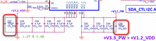
I modify the RX1 & RX2 & TX1 power supply high -frequency wave capacitance
On the TMDS181, 40.2k pullup on DDC_SDA/SCL is out of HDMI spec, need use 47k +/-10%-->we refence Xilinx EVB is set 40.2K OHM.
For pin-strap mode, set TMDS181 TEST/A1 to NC-->I discuss this setting of FPGA Team.
Set TMDS181 EQ_SEL to NC-->I discuss this setting of FPGA Team.
For both DP159 and TMDS181, too many 4.7uF, keep one and replace rest with 0.1uF --> OK! we will modify circuit
FPGA input requires to be AC coupled, but TMDS181 output needs to be 3.3V common mode voltage, so use external 50ohm termination to 3.3V to set the CM. But 50ohm termination and FGPA input termination create double termination so output signal amplitude gets cut in offer. May need to adjust TMDS181 output SWING to compensate-->I discuss this setting of FPGA Team.
Thanks so much for the quick feedback and communication. Let me know how the discussions with the FPGA team goes. I will look into the DDC pullup values.
For pin-strap mode, set TMDS181 TEST/A1 to NC-->I will modify circuit to NC.
Set TMDS181 EQ_SEL to NC-->I will modify circuit to NC.
For both DP159 and TMDS181, too many 4.7uF, keep one and replace rest with 0.1uF -->I will modify circuit to NC.
FPGA input requires to be AC coupled, but TMDS181 output needs to be 3.3V common mode voltage, so use external 50ohm termination to 3.3V to set the CM. But 50ohm termination and FGPA input termination create double termination so output signal amplitude gets cut in offer. May need to adjust TMDS181 output SWING to compensate-->we circuit TMDS181 TMDS 49.9OHM Pull up 3.3V--> AC CAP ---> input FPGA MGT BANK.
Between TMDS181 & FPGA, the characteristics of using AC capacitance isolation DC. We don't think there will be a condition of Create Double Termination. Thank you^^
On the TMDS181, 40.2k pullup on DDC_SDA/SCL is out of HDMI spec, need use 47k +/-10%-->we refence Xilinx EVB is set 40.2K OHM
As per the HDMI spec you need to have a 47k ohm resistor on the DDC lines:
We cannot see what Xilinx is doing internally at these pins, so please consult with them and confirm that they are meeting spec with their reference design.
Between TMDS181 & FPGA, the characteristics of using AC capacitance isolation DC. We don't think there will be a condition of Create Double Termination. Thank you^^
You will still need to math the terminations between the FPGA and the the output to reduce reflections. Tuning may need to be done based off of the internal terminations of the FPGA
FPGA input requires to be AC coupled, but TMDS181 output needs to be 3.3V common mode voltage, so use external 50ohm termination to 3.3V to set the CM. But 50ohm termination and FGPA input termination create double termination so output signal amplitude gets cut in offer. May need to adjust TMDS181 output SWING to compensate-->we circuit TMDS181 TMDS 49.9OHM Pull up 3.3V--> AC CAP ---> input FPGA MGT BANK.
Based off the information provided, it seems that the double termination, and the DDC pull ups have been addressed. Let me know if you need anything else from our end.