This thread has been locked.

If you have a related question, please click the "Ask a related question" button in the top right corner. The newly created question will be automatically linked to this question.

DS125DF111: Retimer for FPGA at Optical Network Unit

Part Number: DS125DF111
Other Parts Discussed in Thread: DS125DF1610, DS100MB203, DS250DF230, USB2ANY, , DS125MB203

Hello Team,

At present, the optical module ONU is directly connected to the SerDes interface of the FPGA,

but the optical sensitivity can only be measured to -31.5dBm (unqualified), and the optical sensitivity is required to reach -33dBm.
I want to use DS125DF111SQ, but I don't know if I can use it, what should I pay attention to?

FPGA model: MPF100T-FCG484E, in fact, the FPGA cannot catch the error of 10E-3 , and the system needs to be shaped by the retimer chip.

Thank you!

  • Hi,

    Do you have any information or measurements on the electrical signal that the DS125DF111 would receive?  The DS125DF111 CTLE can apply up to 33 dB of boost at 6.25 GHz, but this is targeted at equalizing a PCB channel.

    Will signal impairment from an ONU be similar to a PCB channel in that high frequency components of the signal will be attenuated?  Or will an optical signal of -33dBm also have significantly reduced low frequency amplitude?

    Thanks,

    Drew

  • Hello Miller,

    Electrical signal is a Serdes type, at present , we do not measure it eye diagram with DS125DF111. but it seems signal impairment from an ONU-TIA. We only need DS125  do Signal Enhancement. So, do you have any advice? Or do you have some 1in 2out repeat seders chip recommdation?

    Thank you!

  • Hi,

    You can try the DS125DF111.  It has CTLE and DFE to help with impaired signals.  With that said, it's hard to comment on how effective it will be without a better understanding of the electrical signaling.  The DS125DF111 typically works well with common high speed SERDES signaling levels such as those implemented in Ethernet.

    We have IBIS-AMI model that can be used to help increase confidence in the part selection.

    Regarding a 1:2 repeater type device, we have redrivers and retimers that offer this functionality.  For a redriver, a device like DS100MB203 may be suitable.  We don't have 10G retimers offering this (with the exception of DS125DF1610), but our 25G retimers, such as DS250DF230 can be configured to support 1:2 fan out.  Our 25G retimers also support 10G data rates, but will not offer as much CTLE boost at 10G rates as our 10G retimer devices.

    Thanks,

    Drew

  • Hello Miller,
    (1) The attachment is about the schematic diagram and PCB board of the chip application in our company, please help check;
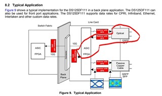
    (2) In addition, our application is shown in the following figure (44 pages of the specification);
    (3) The rate will be switched between 10.315Gb/s (10GEPON) and 9.95328Gb/s (XGS-PON), whether the chip can be adaptive, if there are no empirical parameters;
    (4) In addition, we want to check the eye diagram during the debugging process, can the USB2ANY in the attachment be used?

    Thanks,

    Sheet1.SchDoc

    PCB1.PcbDoc

  • Hi,

    (1) I can provided schematic/layout feeback next week.

    (3) Yes, the retimer can be configured to lock to these two data rates.

    (4) Yes, you can use the USB2ANY and SigCon Architect to view an eye diagram.

    Thanks,

    Drew

  • Hi,

    One follow up thought:

    The DS125DF111 is known to work well with SFP+ optical modules, where electrical signaling is consistent with SFF-8418 electrical specifications.

    As part of the SFF-8418 module receiver specification, there is an eye mask with an eye of at least 0.7UI and 300mVppd.  Do you know how the 10GEPON and XGS-PON electrical signaling will compare?

    Thanks,

    Drew

  • Hello Drew,

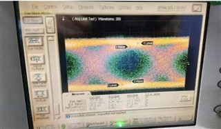
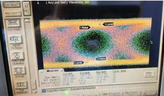
    The 10GEPON and XGS-PON electrical signaling show below.

    XGS-PON

    10GEPON

  • Hi,

    Thanks for sharing scope data.  Is it correct that this is a single ended signal?  If so, it appears your differential signal amplitude would be around 260mVppd.  

    Typically, we target an internal eye of 200mVppd and 0.4UI as recorded by the internal eye monitor of the retimer.  The eye monitor takes eye measurements after the CTLE and DFE stages of the retimer.  This seems to give a small margin to reach the internal eye target for the retimer.  If signal amplitude is the only signal impairment, the retimer CTLE stage can be configured as a limiting amplifier, so this might help with the amplitude.

    With this said, is it possible to do testing with one of our DS125DF111EVM?  This could help to better understand retimer performance in this application before designing a board with the retimer.

    Thanks,

    Drew

  • Hi,

    Please find schematic review information attached.

    1715.Schematic Review Helper.pdf

    Thanks,

    Drew

  • Hello Drew,

    Thank you for your kindly support. And now we have some questions, We want to DS125MB203  to achieve the following functions: input one optical module signal, output two identical signals , in which the rate of the optical module is 1G, 2.5G (actual 2.488G), 10G (there are two kinds of 10Gepon,one is 10.315G, another 10xgpon is 9.953G);

    All of the above rates are required, whether this chip can achieve this function, or you have others for recommenation.

    Thanks!

  • Hi,

    Yes, this device can support these rates.

    Thanks,
    Drew