This thread has been locked.

If you have a related question, please click the "Ask a related question" button in the top right corner. The newly created question will be automatically linked to this question.

TIC10024-Q1: Voltage at INx Pin of TIC10024-Q1

Part Number: TIC10024-Q1

Hi,

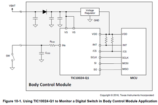
For ground connected switch with following resistances;

Switch Resistance when open, Rsw_open=50 Kohm

Switch Resistance when closed,Rsw_closed=50 ohm

For 10mA wetting current setting, 

Voltage at Inx pin when switch is open= 10mA*50 Kohm=500V.

This exceeds the voltage limit at INx pin which is 40 V maximum.

Can you help with this issue?

  • Hello Bhaskar,

    The maximum voltage on the INx pin will be a diode's drop below the VS supply voltage.  The wetting current circuits are not "constant current" circuits that force a specific amount of current across any value of load resistance.  If they were, you would be correct that the voltage on the INx pin would have to increase to a level greater than the VS supply voltage.

    Instead the wetting current circuits act more like "current limiting" circuits and are basically a Pass FET architecture with a max current limit.  The device operates on the basic principle of Ohm's Law (V=I*R) where V = VS supply voltage (minus a diode's drop), R =  Resistance between INx pin and GND, and I = Current Flow across the resistance between INx pin and GND.

    When the resistance between the INx pin is very large (such as when a switch is open), there will be very little if any wetting current flowing out of the INx pin and the INx pin voltage will be roughly equal to the VS supply voltage minus a diode's drop. 

    However, when the switch is closed and there is a very low resistance between the INx pin and GND such that the current across the resistance would be greater than the configured wetting current limit (1,2,5,10, or 15 mA), then the device will limit the amount of wetting current to this configured level.  Then the INx pin voltage would simply be determined by solving Ohm's Law (V=I*R = Wetting Current * Resistance).

    When the resistance is large enough to allow some wetting current to flow, but not enough to become limited, the amount of wetting current flowing through the resistance will be determined by Ohm's Law (I = V/R = VS supply voltage / Resistance).

    Under no circumstances could the device force enough current to increase the INx pin voltage greater than the VS supply voltage.

    Regards,

    Jonathan

  • Hi Johnathan,

    Thank You for your prompt reply.

    I want to calculate the exact voltage across the INx pin considering the drop across the diode and pass FET of the current limiting circuit. Can you please let me know the maximum forward voltage drop across the diode and on state resistance of pass FET?

    Regards,

    Bhaskar Kafle

  • Hi Bhaskar,

    The voltage drop and on state resistance of the pass FET is not specified nor should be required information because the wetting current is of primary concern for these types of devices.

    The TIC10024-Q1 uses a comparator to detect whether the pin voltage is above one of 4 configurable voltage thresholds (2V, 2.7V, 3V, or 4V). 

    When there is a resistive path to ground allowing current to flow between the INx pin and GND, then the Voltage on the INx pin will be:

    Vinx = Req x Iwett (where Req is the equivalent resistance and Iwett is the wetting current level)

    When there is not a resistive path to ground, or the resistance value is large enough to prevent the Vinx voltage from being below the comparator's threshold, the device will only know that the Vinx voltage is above the threshold. 

    This device can only inform you whether the voltage is above or below the comparator threshold and this is a product of the amount of current flowing across the resistive load between the INx pin and GND. 

    Regards,

    Jonathan

  • Hi Johnathan,

    I had query regarding VCSI_DROP_OPEN and VCSI_DROP_CLOSED parameters in the datasheet. Should we consider these values during Input voltage calculation at INx pin for battery connected pins.

    Regards,

    Bhaskar Kafle 

  • Hi Bhaskar,

    Thanks for your question. Today is a holiday in the US. Jonathan will be back early next week to provide a comment here. Thanks for your patience. 

    Regards, 
    Eric Schott

  • Hi Bhaskar,

    Yes.  The Current Sink Circuit sits between the INx pin and GND and there is a small voltage drop across the transistors that make up this circuit preventing voltage at the INx pin from being equal to GND.  Therefore, when you are using battery connected switches, you should factor in this voltage drop when determining your threshold levels.

    The datasheet specifies a maximum level that is associated with the worst case value based on semiconductor manufacturing process variations, voltage and temperature, and operating conditions and some statistical margin.  Therefor the typical value will be less than this max value and you should never see this guaranteed max value. I have personally measured this on many units to be closer to the 300mV value under nominal conditions, but you will need to account for a value up to the datasheet max limit.

    However, the TIC10024-Q1 comparator's lowest detection threshold is 2V which is above the max VCSI_DROP value so this should not be an issue.

    Regards,

    Jonathan

  • Hi Jonathan,

    Thank You for explanation.

    Can you please help me calculate the voltage at INx pin for battery (Vbat=18V) connected pin when the switch is closed for switch resistance of 50ohm and 15mA wetting current setting considering VCSI_DROP_CLOSED.

    Regards,

    Bhaskar Kafle

  • Hi Bhaskar,

    The INx pin voltage will be the voltage drop across the switch resistance subtracted from the battery voltage.

    INx = Vbat - (Wetting Current * Switch Resistance)

    INx = 18 - (0.015 * 50) = 17.25V

    With battery connected switches, you will need larger switch resistance values in order to get the INx voltage low enough to drop below a comparator threshold.  This is because the battery voltage is a fixed voltage level making the INx voltage the result of the voltage drop created by the current flowing through the switch resistance.  This is simply Ohm's Law (V = I * R).

    Likewise in a current source configuration where the switches are ground based, the fixed voltage level becomes GND or 0V and the INx pin voltage is simply the higher side of the voltage created by the current flowing through the switch resistance.  In this case lower switch resistances are needed.

    The VCSI_DROP_CLOSED parameter is only of concern when you have resistances that would place the INx pin voltage around or below this specified level because this parameter is essentially a ground offset value.  For example the maximum resistance value for a full 15mA wetting current across an 18V drop would be 1200 ohms (18/0.015 = 1200).  If the switch resistance was greater than 1200 ohms or the voltage drop was less than 18V, the wetting current would be less than 15mA. 

    The VCSI_DROP_CLOSED spec means that the device may not be able to pull the INx pin voltage below this max level in some operating conditions even if the switch resistance is sized appropriately.

    Regards,

    Jonathan