This thread has been locked.

If you have a related question, please click the "Ask a related question" button in the top right corner. The newly created question will be automatically linked to this question.

DP83TC814S-Q1: About LED Configuration Question

Part Number: DP83TC814S-Q1
Other Parts Discussed in Thread: DP83TC812EVM-MC

Tool/software:

Hello TI Team,

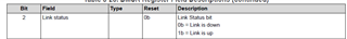
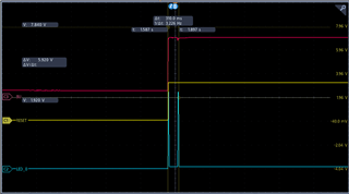
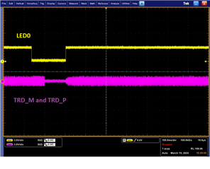
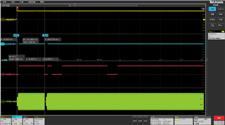
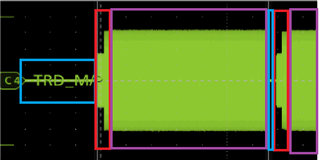
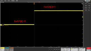
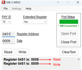
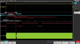
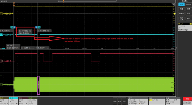
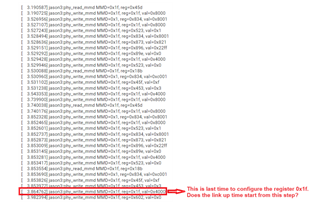
LED0 has the function of Link-OK indication.

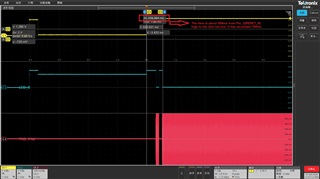
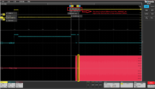
Does it output blink_rate when it links OK?

Now, we can't measure the blink rate when it links ok.

How to configurate the function?

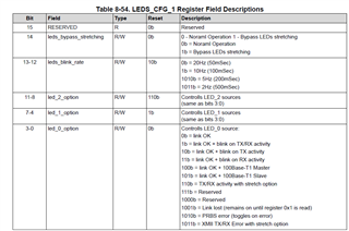
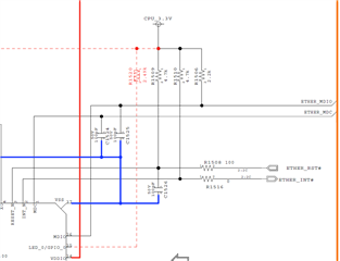
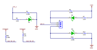
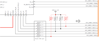
Below is our schematic:

Best Regards!

  • Hi Jingkun,

    Can you provide a screenshot of your LED0 schematic?

    By default, LED0 should typically be HIGH when link is up and LOW when link is down.

    If it is blinking and you have not changed the register settings, it may be linking up and linking down. Can you read register 0x1 multiple times to confirm the link status?

    You can configure LED0 to blink by setting the LEDS_CFG_1 registers as shown above. Register settings are changed via MDIO/MDC on the DP83TC814. 

    Best regards,

    Melissa

  • Hello Melissa,

    Below is  LED0 schematic.

    If the LED0 is blinking, it indicates that PHY is linking.

    If it links up, LED0 will output high. Is it right?

    Best Regards!

    Wang Jingkun

  • HI Jingkun,

    I don't see an LED connected to the LED0 pin on the DP83TC814. Is this correct?

    Yes, if there is link, LED0 will output high.

    Best regards,

    Melissa

  • Hello Melissa,

    Yes, it doesn't have an LED connected to the LED0 pin.

    Best Regards!

  • Hello Melissa,

    When LED0 pin added the pull up resistance (2.49k) to set the DUT as master mode.

    I read the register 0x1,  the bit2=1,  but the LED0 pin didn't output high.

    Why?

    Best Regards!

  • Hi Jingkun,

    If you probe LED1 during link up, what do you see?

    Can you read back registers 0x0-0x1F and 0x45D? 

    Best regards,

    Mellissa

  • Hi Mellissa,

    Below is read back register's value:

    0x00 : 0x2100
    0x01 : 0x0065
    0x02 : 0x2000
    0x03 : 0xa261
    0x04 : 0x0001
    0x05 : 0x0000
    0x06 : 0x0000
    0x07 : 0x2001
    0x08 : 0x0000
    0x09 : 0x0000
    0x0A : 0x0100
    0x0B : 0x0000
    0x0C : 0x0000
    0x0D : 0x401f
    0x0E : 0x0000
    0x0F : 0x0000
    0x10 : 0x0205
    0x11 : 0x010b
    0x12 : 0xe400
    0x13 : 0x0000
    0x14 : 0x0000
    0x15 : 0x0000
    0x16 : 0x0100
    0x17 : 0x0000
    0x18 : 0x1a25
    0x19 : 0x0c00
    0x1A : 0x0000
    0x1B : 0x0000
    0x1C : 0x0000
    0x1D : 0x0000
    0x1E : 0x0000
    0x1F : 0x0000
    0x0450: 0x2610
    0x0451: 0x0000
    0x045D: 0x62c0

    Another issue, 

    Do you have the link up time test result in the DP83TC812EVM-MC?

    The OPEN Alliance Automotive Ethernet ECU Test requirement as below:

    Below is test from DP83TC812EVM-MC:

    It has exceeded 100ms.

    Best Regards!

  • Hi Jingkun,

    Can you probe LED1 as well? This should also indicate link activity, I want to see if it is similar to the LED0 waveform you are seeing. 

    Below is read back register's value:

    Thank you providing this. The registers look as expected and the strap register 0x45D says you are correctly strapped into master mode. 

    Do you have the link up time test result in the DP83TC812EVM-MC?

    The OPEN Alliance Automotive Ethernet ECU Test requirement as below:

    Yes, we have an Interopability repot available from C&S. We typically give this out to ur customers with NDA, can you reach out to your local TI Field Representative for this?

    Below is test from DP83TC812EVM-MC:

    It has exceeded 100ms.

    This LED0 waveform does not look correct. To debug, can you (1) measure LED1 and (2) try depopulating the pull up resistor on LED0 and measuring the waveform again, and (3) measuring TRD_P and TRD_M with a differential probe?

    While LED0 can be used to indicate link status, it should not be used to measure the link up time because there is some delay.

    The Open Alliance Test house has a more precise test setup to measure the time that is a bit difficult to replicate. However, you can get an estimate by using a differential probe to measure across TRD_M and TRD_P.

    This is what my waveform look like:

    Best regards,

    Melissa

  • Hello Melissa,

    This LED0 waveform does not look correct. To debug, can you

    (1) measure LED1 

    ---> Add LED1 in the waveform

    (2) try depopulating the pull up resistor on LED0 and measuring the waveform again

    ---> It was used DP83TC812EVM-MC for testing. It has the pull up resistor.

    (3) measuring TRD_P and TRD_M with a differential probe?

    ---> OK.

    Below is test result:

    I don't know how to judge the link up time from the TRD_P/M.

    Could you add the comment in the waveform?

    Best Regards!

  • Hi Jingkun,

    Thanks for providing this information! 

    It looks like from the TRD_P/TRD_M waveform it is linking up twice. 

    In the DP83TC812MC EVM and in the SW drivers we provide, there is an Open Alliance Compliance initialization sequence, which restarts the PHY (0x1F=0x4000) and restarts the link up process, so it is expected. 

    I have circled link DOWN in blue, link UP in purple, and link training/link up in red. Link up timer begins with the sending of PAM3 idle signals (in red).

    For the LED0 waveform, it looks like polairty is being inverted to active LOW. Can you 

    (1) Confirm that no HW/SW changes have been made to the EVM. Did you replace the 812 with 814?

    (2) provide a picture of your DP83TC812MC-EVM? I want to check strap settings.

    (3) Try writing 0x451[0]=1 to invert the polarity to see if that fixes the polarity

    Best regards,

    Melissa

  • Hello Melissa,

    (1) Confirm that no HW/SW changes have been made to the EVM. Did you replace the 812 with 814?

    ---> It doesn't have any changes in the EVM.  We didn't replace the 812 with 814.

    (2) provide a picture of your DP83TC812MC-EVM? I want to check strap settings.

    ---> Please check below picture:

    (3) Try writing 0x451[0]=1 to invert the polarity to see if that fixes the polarity

    ---> The polarity inverted when writing 0x451[0]=1.  We find that LED_0 is active low when it is in master mode. And LED_0 is active high when it is in slave mode.  We don't do any configuration.  Is this consistent with TI's design expectations?

    Best Regards!

  • Hi Jingkun,

    Apologies for the confusion. 

    If LED0 is pulled HIGH (strapped into master mode), it will be Active LOW. 

    If LED0 is NC or pulled LOW, it will be Active HIGH.

    If you leave LED0 NC or pulled LOW, it will still be Active HIGH even if you program the PHY to Master Mode via register writes.

    Best regards,

    Melissa

  • Hello Melissa,

    I got the link up time test report.

    Below questions, could you help to confirm again?

    1. The DUT’s PHY configuration must be finished within 20ms after reset.  Do you give us the configuration document?

    2. DUT shall wait until the PHY indicates an active link and stop timer t0.  How to get the info that PHY indicates an active link?  Read the register 0x001[2]?

    Best Regards!

  • Hi Jingkun,

    1. The DUT’s PHY configuration must be finished within 20ms after reset.  Do you give us the configuration document?

    This is provided in the test report, section 9.3 Configuration Script.

    The registers used for configuration are also found here in section 3: https://www.ti.com/lit/an/snla389b/snla389b.pdf?ts=1719362666393 

    2. DUT shall wait until the PHY indicates an active link and stop timer t0.  How to get the info that PHY indicates an active link?  Read the register 0x001[2]?

    There is some latency and delay in reading 0x001[2], I don't believe this will work. I will need to check how this is measured and get back to you by the end of the week.

    Is there a particular reason you want to measure t0? Are you testing a link partner that is not part of our test report?

    Best regards,

    Melissa

  • Hello Melissa,

    Now, we are testing the link up time. But the test result is more than 100ms.

    We recorded the link up time is from reset release to reading the register 0x001[2].

    We test the link partner :  master is DP83TC814SRHARQ1 and the slave is DP83TC814SRHARQ1.

    So we want to know TI using which signal as the indication an active link.

    Best Regards!

  • Hi Jingkun,

    If it is your custom board, can you (1) check that you are programming the Open Alliance init script and (2) LED and TRD_P/TRD_M waveforms?

    The Init script can be found here for Master and Slave modes in section 3: https://www.ti.com/lit/an/snla389b/snla389b.pdf?ts=1719511922160 

    From the waveforms you provided, the link up time is <100ms on the TI EVMs. 

    Best regards,

    Melissa

  • Hello Melissa,

    • Are you measuring link up time on your custom board?     
      --> Yes. We are measuring link up time on our board.
    • Are you using our linux or RTOS driver? (https://github.com/TexasInstruments/ti-ethernet-software/tree/main ) 
      --> Our SW team is confirming.
    •  (2) LED and TRD_P/TRD_M waveforms
    • From the waveforms you provided, the link up time is <100ms on the TI EVMs.
      --->It has two red box, it means that it has twice link. Does TI use the time that RESET signal high to the first red box for link up time?

            If it measures to the second red box time, it also is more than 100ms.

    1. There is some latency and delay in reading 0x001[2], I don't believe this will work. I will need to check how this is measured and get back to you by the end of the week.

    --> Could you give us the confirm result that how this is measured?

    2. About the test report, it has some questions, please help to confirm:

    2-1) About the Step 1, does the soft/hard reset mean the register 0x1F[15-14]? Or the pin 3 RESET_N?


    2-2) About the Step 3, the t0 is after finished configuration. Doesn't the link up time include the time spent on configuration?

    Best Regards!

  • Hi Jingkun,

    It seems like the 814s on your custom board is linking up within the correct time. I do not see a problem here from the waveforms you provided. 

    ...

    --->It has two red box, it means that it has twice link. Does TI use the time that RESET signal high to the first red box for link up time?
          If it measures to the second red box time, it also is more than 100ms.

    The linkup time is only the 2nd red box, not the 1st red box.

    2-1) About the Step 1, does the soft/hard reset mean the register 0x1F[15-14]? Or the pin 3 RESET_N?


    1. There is some latency and delay in reading 0x001[2], I don't believe this will work. I will need to check how this is measured and get back to you by the end of the week.

    --> Could you give us the confirm result that how this is measured?

    C&S (official test house) uses register 0x133. However, they some advanced automated setup that measures this with only a microsecond delay. It is hard to replicate. We typically measure at TI by looking at the TRD_P and TRD_M waveforms which provide a good estimate.

    2-1) About the Step 1, does the soft/hard reset mean the register 0x1F[15-14]? Or the pin 3 RESET_N?


    Hard reset is 0x1F=0x8000

    Soft reset is 0x1F=0x4000

    2-2) About the Step 3, the t0 is after finished configuration. Doesn't the link up time include the time spent on configuration?

    For T0, they start the timer after reset in the software and stop the timer after config is done. The requirement for this is 20ms. However, C&S has a advanced automated setup with microsecond delay to measure. It is hard to replicate.

    The passing report we forwarded to you shows we have already passed this spec before, since we have passed IOP21. The config time is unrelated to the link partner. 

    Best regards,

    Melissa

  • Hello Melissa,

    --->It has two red box, it means that it has twice link. Does TI use the time that RESET signal high to the first red box for link up time?
          If it measures to the second red box time, it also is more than 100ms.

    The linkup time is only the 2nd red box, not the 1st red box.

    --> The time is about 556ms from Pin_3(RESET_N) high to the 2nd red box. It has exceeded 100ms.

    So we don't know the resetting PHY means that Pin_3 (RESET_N) changes from low to high, or it means resetting the register.

    If the reset PHY means Pin_3 (RESET_N) changes from low to high, the link up time of demo also exceeded the SPEC requirement.

    Are you base in China? If yes, could you have a talk via phone?

    Below is my phone number:18030086702.

    Best Regards!

  • Hi Jingkun,

    Can you confirm what driver is being used and provide the driver file aswell?

    --> The time is about 556ms from Pin_3(RESET_N) high to the 2nd red box. It has exceeded 100ms.

    It seems there has been some confusion, I was talking about this image where I have drawn red boxes, not the one you've showed above:

    The link up time in this green waveform is the 2nd red box.

    In the new image below, the link up time is the yellow box I have drawn below. 

    On our EVM it should be measured from the register write, not the pin. For future reference hard reset is 0x1F=0x8000 and soft reset is 0x1F=0x4000.

    For your board, I need to confirm in the software driver what register writes are being done after reset. 

    If there is still some confusion we can setup a meeting, please reach out to your local Field Representative to set this up. I am based in the PST Time Zone. 

    Best regards,

    Melissa

  • Hello Melissa: 

    It seems there has been some confusion, I was talking about this image where I have drawn red boxes, not the one you've showed above:

    --> Sorry, I used the wrong picture. Below is demo test result:

    The time is about 556ms from Pin_3(RESET_N) high to the 2nd red box. It has exceeded 100ms.

    On our EVM it should be measured from the register write, not the pin. For future reference hard reset is 0x1F=0x8000 and soft reset is 0x1F=0x4000.

    --> It means that the link up time is from register 0x1F=0x8000 or 0x1F=0x4000 to 0x133[12] =1.  Is it right?

    Best Regards!

  • Hi Jingkun,

    Could you provide the software driver being used for your custom board?

    The link up time is the purple time, from the beginning of PAM3 idle signals to the link up. The flat signal indicates that the PHY has been reset in the SW and link is restarting. 

    Best regards,

    Melissa

  • Hello Melissa,

    Below is configuration list after Pin_3(RESET_N)=High:

    [    3.190587] jason3:phy_read_mmd MMD=0x1f, reg=0x45d
    [    3.190725] jason3:phy_write_mmd MMD=0x1f, reg=0x1f, val=0x8000
    [    3.526956] jason3:phy_write_mmd MMD=0x1, reg=0x834, val=0x8001
    [    3.527107] jason3:phy_write_mmd MMD=0x1f, reg=0x1f, val=0x8000
    [    3.527243] jason3:phy_write_mmd MMD=0x1f, reg=0x523, val=0x1
    [    3.528494] jason3:phy_write_mmd MMD=0x1f, reg=0x834, val=0x8001
    [    3.528636] jason3:phy_write_mmd MMD=0x1f, reg=0x873, val=0x821
    [    3.529151] jason3:phy_write_mmd MMD=0x1f, reg=0x896, val=0x22ff
    [    3.529292] jason3:phy_write_mmd MMD=0x1f, reg=0x89e, val=0x0
    [    3.529428] jason3:phy_write_mmd MMD=0x1f, reg=0x1f, val=0x4000
    [    3.529946] jason3:phy_write_mmd MMD=0x1f, reg=0x523, val=0x0
    [    3.530088] jason3:phy_read_mmd MMD=0x1f, reg=0x18b
    [    3.530960] jason3:phy_write_mmd MMD=0x1, reg=0x834, val=0xc001
    [    3.531102] jason3:phy_write_mmd MMD=0x1f, reg=0x45f, val=0xf
    [    3.531238] jason3:phy_write_mmd MMD=0x1f, reg=0x453, val=0x3
    [    3.543353] jason3:phy_write_mmd MMD=0x1f, reg=0x1f, val=0x4000
    [    3.739900] jason3:phy_write_mmd MMD=0x1f, reg=0x1f, val=0x8000
    [    3.740038] jason3:phy_read_mmd MMD=0x1f, reg=0x45d
    [    3.740176] jason3:phy_write_mmd MMD=0x1f, reg=0x1f, val=0x8000
    [    3.852328] jason3:phy_write_mmd MMD=0x1, reg=0x834, val=0x8001
    [    3.852465] jason3:phy_write_mmd MMD=0x1f, reg=0x1f, val=0x8000
    [    3.852601] jason3:phy_write_mmd MMD=0x1f, reg=0x523, val=0x1
    [    3.852737] jason3:phy_write_mmd MMD=0x1f, reg=0x834, val=0x8001
    [    3.852873] jason3:phy_write_mmd MMD=0x1f, reg=0x873, val=0x821
    [    3.853009] jason3:phy_write_mmd MMD=0x1f, reg=0x896, val=0x22ff
    [    3.853145] jason3:phy_write_mmd MMD=0x1f, reg=0x89e, val=0x0
    [    3.853281] jason3:phy_write_mmd MMD=0x1f, reg=0x1f, val=0x4000
    [    3.853417] jason3:phy_write_mmd MMD=0x1f, reg=0x523, val=0x0
    [    3.853554] jason3:phy_read_mmd MMD=0x1f, reg=0x18b
    [    3.853690] jason3:phy_write_mmd MMD=0x1, reg=0x834, val=0xc001
    [    3.853826] jason3:phy_write_mmd MMD=0x1f, reg=0x45f, val=0xf
    [    3.853972] jason3:phy_write_mmd MMD=0x1f, reg=0x453, val=0x3
    [    3.864762] jason3:phy_write_mmd MMD=0x1f, reg=0x1f, val=0x4000
    [    3.982394] jason3:phy_write_mmd MMD=0x1f, reg=0x602, val=0x0

    Best Regards!

  • Hi Jingkun,

    Yes, linkup would start from the last step. 

    Best regards,

    Melissa 

  • Hello Melissa,

    1.Is there a problem with our software driver?

    2.Could you explain the difference of Pin_3(RESET_N),  0x1f[15] Software Global Reset(Hardware reset) and the 0x1f[14] Digital Rest (Software Restart) ?

    3.Are the functions of Pin_3 (RESET_N) and 0x1f[15] Software Global Reset (Hardware reset) exactly the same? 

    4.Can we cancel the control of Pin_3 (RESET_N)?

    Best Regards!

  • Hi Jingkun,

    I am currently out on vacation today and will provide a full response tomorrow. Are you able to provide the full code file?

    Best regards,

    Melissa

  • Hello Melissa,

    Below is full code file, please find it!

    // SPDX-License-Identifier: GPL-2.0
    /* Driver for the Texas Instruments DP83TC812 PHY
     * Copyright (C) 2021 Texas Instruments Incorporated - http://www.ti.com/
     */
    /* 01/17/2024 Alvaro Reyes (a-reyes1@ti.com)
    * Updated Open Alliance script for the 812 in both Master and Slave
    * Added SQI, TDR, and Forced-Master/Slave features
     * 
     * 02/08/2024 Alvaro Reyes (a-reyes1@ti.com)
     * 
     * New Global Variables
     * 
     * Updated Functions:
     * dp83812_reset
     * dp83812_phy_reset
     * dp83812_chip_init
     * dp83812_config_init
     * dp83812_config_aned
     * dp83812_probe
     */
    
    #include <linux/ethtool.h>
    //#include <linux/ethtool_netlink.h>
    #include <linux/etherdevice.h>
    #include <linux/kernel.h>
    #include <linux/mii.h>
    #include <linux/mdio.h>
    #include <linux/module.h>
    #include <linux/of.h>
    #include <linux/phy.h>
    #include <linux/netdevice.h>
    #include <linux/bitops.h>
    
    #define DP83TC812_CS2_0_PHY_ID			0x2000a271
    #define DP83TC813_CS2_0_PHY_ID			0x2000a211
    #define DP83TC814_CS2_0_PHY_ID			0x2000a261
    
    #define MMD1F							0x1f
    #define MMD1							0x1
    
    #define DP83TC812_STRAP					0x45d
    #define MII_DP83TC812_SGMII_CTRL		0x608
    #define SGMII_CONFIG_VAL				0x027B
    #define MII_DP83TC812_RGMII_CTRL		0x600
    #define MII_DP83TC812_INT_STAT1			0x12
    #define MII_DP83TC812_INT_STAT2			0x13
    #define MII_DP83TC812_INT_STAT3			0x18
    #define MII_DP83TC812_RESET_CTRL		0x1f
    #define MMD1_PMA_CTRL_2					0x1834
    #define DP83TC812_TDR_CFG5				0x0306
    #define DP83TC812_CDCR					0x1E
    #define TDR_DONE						BIT(1)
    #define TDR_FAIL						BIT(0)
    #define DP83TC812_TDR_TC1				0x310
    #define DP83TC812_TDR_START_BIT			BIT(15)	
    #define DP83TC812_TDR_half_open_det_en 	BIT(4)
    #define BRK_MS_CFG						BIT(14)
    #define HALF_OPEN_DETECT				BIT(8)
    #define PEAK_DETECT						BIT(7)
    #define PEAK_SIGN						BIT(6)
    
    #define DP83TC812_HW_RESET				BIT(15)
    #define DP83TC812_SW_RESET				BIT(14)
    
    /* INT_STAT1 bits */
    #define DP83TC812_RX_ERR_CNT_HALF_FULL_INT_EN	BIT(0)
    #define DP83TC812_TX_ERR_CNT_HALF_FULL_INT_EN	BIT(1)
    #define DP83TC812_MS_TRAIN_DONE_INT_EN			BIT(2)
    #define DP83TC812_ESD_EVENT_INT_EN				BIT(3)
    #define DP83TC812_LINK_STAT_INT_EN				BIT(5)
    #define DP83TC812_ENERGY_DET_INT_EN				BIT(6)
    #define DP83TC812_LINK_QUAL_INT_EN				BIT(7)
    
    /* INT_STAT2 bits */
    #define DP83TC812_JABBER_INT_EN			BIT(0)
    #define DP83TC812_POL_INT_EN			BIT(1)
    #define DP83TC812_SLEEP_MODE_INT_EN		BIT(2)
    #define DP83TC812_OVERTEMP_INT_EN		BIT(3)
    #define DP83TC812_FIFO_INT_EN			BIT(4)
    #define DP83TC812_PAGE_RXD_INT_EN		BIT(5)
    #define DP83TC812_OVERVOLTAGE_INT_EN	BIT(6)
    #define DP83TC812_UNDERVOLTAGE_INT_EN	BIT(7)
    
    /* INT_STAT3 bits */
    #define DP83TC812_LPS_INT_EN			BIT(0)
    #define DP83TC812_WUP_INT_EN			BIT(1)
    #define DP83TC812_WAKE_REQ_INT_EN		BIT(2)
    #define DP83TC811_NO_FRAME_INT_EN		BIT(3)
    #define DP83TC811_POR_DONE_INT_EN		BIT(4)
    #define DP83TC812_SLEEP_FAIL_INT_EN		BIT(5)
    
    /* RGMII_CTRL bits */
    #define DP83TC812_RGMII_EN				BIT(3)
    
    /* SGMII CTRL bits */
    #define DP83TC812_SGMII_AUTO_NEG_EN		BIT(0)
    #define DP83TC812_SGMII_EN				BIT(9)
    
    /* Strap bits */
    #define DP83TC812_MASTER_MODE			BIT(9)
    #define DP83TC812_RGMII_IS_EN			BIT(7)
    
    /* RGMII ID CTRL */
    #define DP83TC812_RGMII_ID_CTRL			0x602
    #define DP83TC812_RX_CLK_SHIFT			BIT(1)
    #define DP83TC812_TX_CLK_SHIFT			BIT(0)
    
    /*SQI Status bits*/
    #define DP83TC812_dsp_reg_71			0x871
    #define MAX_SQI_VALUE					0x7
    
    enum DP83TC812_chip_type {
    	DP83TC812_CS1 = 0,
    	DP83TC812_CS2,
    	DP83TC813_CS2,
    	DP83TC814_CS2,
    };
    
    struct DP83TC812_init_reg {
    	int	reg;
    	int	val;
    };
    
    static const struct DP83TC812_init_reg DP83TC812_master_cs2_0_init[] = {
    	{0x001F, 0x8000},
    	{0x0523, 0x0001},
    	{0x0834, 0xC001},
    	{0x081C, 0x0FE2},
    	{0x0872, 0x0300},
    	{0x0879, 0x0F00},
    	{0x0806, 0x2952},
    	{0x0807, 0x3361},
    	{0x0808, 0x3D7B},
    	{0x083E, 0x045F},
    	{0x0834, 0x8000},
    	{0x0862, 0x00E8},
    	{0x0896, 0x32CB},
    	{0x003E, 0x0009},
    	{0x001F, 0x4000},
    	{0x0523, 0x0000},
    };
    
    static const struct DP83TC812_init_reg DP83TC812_slave_cs2_0_init[] = {
    	{0x001F, 0x8000},
    	{0x0523, 0x0001},
    	{0x0834, 0x8001},
    	{0x0873, 0x0821},
    	{0x0896, 0x22FF},
    	{0x089E, 0x0000},
    	{0x001F, 0x4000},
    	{0x0523, 0x0000},
    };
    
    static const struct DP83TC812_init_reg DP83TC812_tdr_config_init[] = {
    	{0x523, 0x0001},
    	{0x827, 0x4800},
    	{0x301, 0x1701},
    	{0x303, 0x023D},
    	{0x305, 0x0015},
    	{0x306, 0x001A},
    	{0x01f, 0x4000},
    	{0x523, 0x0000},
    	{0x01f, 0x0000},
    };
    
    struct DP83TC812_private {
    	int chip;
    	bool is_master;
    	bool is_rgmii;
    	bool is_sgmii;
    	struct mutex mutex;
    };
    
    #if IS_ENABLED(CONFIG_OF_MDIO)
    static int DP83TC812_get_int_delay_property(struct device *dev, const char *name)
    {
    	s32 int_delay;
    	int ret;
    
    	ret = device_property_read_u32(dev, name, &int_delay);
    	if (ret)
    		return ret;
    
    	return int_delay;
    }
    #else
    static int DP83TC812_get_int_delay_property(struct device *dev, const char *name)
    {
    	return -EINVAL;
    }
    #endif
    
    
    s32 DP83TC812_get_internal_delay(struct phy_device *phydev, struct device *dev,
    			   const int *delay_values, int size, bool is_rx)
    {
    	s32 delay;
    	int i;
    
    	if (is_rx) {
    		delay = DP83TC812_get_int_delay_property(dev, "rx-internal-delay-ps");
    		if (delay < 0 && size == 0) {
    			if (phydev->interface == PHY_INTERFACE_MODE_RGMII_ID ||
    			    phydev->interface == PHY_INTERFACE_MODE_RGMII_RXID)
    				return 1;
    			else
    				return 0;
    		}
    
    	} else {
    		delay = DP83TC812_get_int_delay_property(dev, "tx-internal-delay-ps");
    		if (delay < 0 && size == 0) {
    			if (phydev->interface == PHY_INTERFACE_MODE_RGMII_ID ||
    			    phydev->interface == PHY_INTERFACE_MODE_RGMII_TXID)
    				return 1;
    			else
    				return 0;
    		}
    	}
    
    	if (delay < 0)
    		return delay;
    
    	if (delay && size == 0)
    		return delay;
    
    	if (delay < delay_values[0] || delay > delay_values[size - 1]) {
    		phydev_err(phydev, "Delay %d is out of range\n", delay);
    		return -EINVAL;
    	}
    
    	if (delay == delay_values[0])
    		return 0;
    
    	for (i = 1; i < size; i++) {
    		if (delay == delay_values[i])
    			return i;
    
    		/* Find an approximate index by looking up the table */
    		if (delay > delay_values[i - 1] &&
    		    delay < delay_values[i]) {
    			if (delay - delay_values[i - 1] <
    			    delay_values[i] - delay)
    				return i - 1;
    			else
    				return i;
    		}
    	}
    
    	phydev_err(phydev, "error finding internal delay index for %d\n",
    		   delay);
    
    	return -EINVAL;
    }
    
    static int DP83TC812_set_bits_mmd(struct phy_device *phydev, int devad,
    		u32 regnum, u16 val)
    {
    	struct DP83TC812_private *DP83TC812 = phydev->priv;
    	int ret, new;
    	
    	mutex_lock(&DP83TC812->mutex);
    
    	ret = phy_read_mmd(phydev, devad, regnum);
    	if (ret < 0)
    		goto out;
    	
    	new = ret | val;
    	if(new == ret){
    		ret = 0;
    		goto out;
    	}
    
    	ret = phy_write_mmd(phydev, devad, regnum, new);
    
    out:
    	mutex_unlock(&DP83TC812->mutex);
    
    	return ret < 0 ? ret : 0;
    }
    
    static int DP83TC812_read_straps(struct phy_device *phydev)
    {
    	struct DP83TC812_private *DP83TC812 = phydev->priv;
    	int strap;
    
    	strap = phy_read_mmd(phydev, MMD1F, DP83TC812_STRAP);
    	if (strap < 0)
    		return strap;
    
    	if (strap & DP83TC812_MASTER_MODE)
    		DP83TC812->is_master = true;
    
    	if (strap & DP83TC812_RGMII_IS_EN)
    		DP83TC812->is_rgmii = true;
    	return 0;
    };
    
    static int DP83TC812_reset(struct phy_device *phydev, bool hw_reset)
    {
    	int ret;
    
    	if (hw_reset)
    		ret = phy_write_mmd(phydev, MMD1F, MII_DP83TC812_RESET_CTRL,
    				DP83TC812_HW_RESET);
    	else
    		ret = phy_write_mmd(phydev, MMD1F, MII_DP83TC812_RESET_CTRL,
    				DP83TC812_SW_RESET);
    
    	if (ret)
    		return ret;
    
    	mdelay(100);
    
    	return 0;
    }
    
    static int DP83TC812_phy_reset(struct phy_device *phydev)
    {
    	int err;
    	int ret;
    
    	err = phy_write_mmd(phydev, MMD1F, MII_DP83TC812_RESET_CTRL, DP83TC812_HW_RESET);
    	if (err < 0)
    		return err;
    
    	ret = DP83TC812_read_straps(phydev);
    	if (ret)
    		return ret;
    
    	return 0;
    }
    
    static int DP83TC812_write_seq(struct phy_device *phydev, const struct
    				DP83TC812_init_reg *init_data, int size)
    {
    	int ret;
    	int i;
    
    	for (i = 0; i < size; i++) {
    		ret = phy_write_mmd(phydev, MMD1F, init_data[i].reg,
    					init_data[i].val);
    		if (ret)
    			return ret;
    	}
    	return 0;
    }
    
    #if 0
    static int DP83TC812_setup_master_slave(struct phy_device *phydev)
    {	
    	switch(phydev->master_slave_set)
    	{
    		case MASTER_SLAVE_CFG_MASTER_FORCE:
    		case MASTER_SLAVE_CFG_MASTER_PREFERRED:
    			return phy_write_mmd(phydev, MMD1, 0x0834, 0xC001);
    		case MASTER_SLAVE_CFG_SLAVE_FORCE:
    		case MASTER_SLAVE_CFG_SLAVE_PREFERRED:
    			return phy_write_mmd(phydev, MMD1, 0x0834,0x8001);
    	case MASTER_SLAVE_CFG_UNKNOWN:
    	case MASTER_SLAVE_CFG_UNSUPPORTED:	
    	default:
    		return 0;	
    	}
    }
    #endif
    
    #if 0
    static int DP83TC812_read_master_slave(struct phy_device *phydev)
    {
    	int ctrl2 = phy_read_mmd(phydev, MMD1, MMD1_PMA_CTRL_2);
    
    	if (ctrl2 < 0)
    		return ctrl2;
    	
    	if (ctrl2 & BRK_MS_CFG){
    		phydev->master_slave_get = MASTER_SLAVE_CFG_MASTER_FORCE;
    		phydev->master_slave_state = MASTER_SLAVE_STATE_MASTER;
    		return 1;
    	} else {
    		phydev->master_slave_get = MASTER_SLAVE_CFG_SLAVE_FORCE;
    		phydev->master_slave_state = MASTER_SLAVE_STATE_SLAVE;
    		return 0;
    	}
    
    	return 0;
    }
    #endif
    
    static int DP83TC812_read_status(struct phy_device *phydev)
    {
    	int ret;
    
    	ret = genphy_read_status(phydev);
    	if (ret)
    		return ret;
    	
    //	ret = DP83TC812_read_master_slave(phydev);
    	
    	return 0;
    }
    
    #if 0
    static int DP83TC812_sqi(struct phy_device *phydev){
    	int sqi;
    
    	sqi = phy_read_mmd(phydev,MMD1F,DP83TC812_dsp_reg_71);
    
    	if(sqi < 0){
    		printk("Error: Invalid Value.\n");
    		return sqi;
    	}
    
    	sqi = (sqi >> 1) & 0x7;
    
    	return sqi;
    }
    
    static int DP83TC812_sqi_max(struct phy_device *phydev){
    	return MAX_SQI_VALUE;
    }
    
    static int DP83TC812_cable_test_start(struct phy_device *phydev){
    	
    	if(DP83TC812_read_master_slave(phydev)) 
    		printk("PHY is set as Master.\n");
    	else
    		printk("PHY is set as Slave.\n");
    	
    	DP83TC812_write_seq(phydev, DP83TC812_tdr_config_init, ARRAY_SIZE(DP83TC812_tdr_config_init));
    
    	phy_write_mmd(phydev,MMD1F,DP83TC812_CDCR, DP83TC812_TDR_START_BIT);
    
    	msleep(100);
    
    	return 0;
    }
    
    static int DP83TC812_cable_test_report_trans(u32 result) {
    	int length_of_fault;
    	if (result == 0) {
    		printk("No Fault Detected. \n");
    		return ETHTOOL_A_CABLE_RESULT_CODE_OK;
    	} 
    	else if (result & PEAK_DETECT) {
    		length_of_fault = (result & 0x3F);
    
    		// If Cable is Open
    		if(result & PEAK_SIGN){	
    
    			/*if(result & HALF_OPEN_DETECT){
    				printk("Half Open Cable Detected\n");
    				printk("Length of Fault: %d Meters\n",length_of_fault);
    				return ETHTOOL_A_CABLE_RESULT_CODE_OPEN;
    			} */				
    			printk("Open Cable Detected\n");
    			printk("Length of Fault: %d Meters\n",length_of_fault);
    			return ETHTOOL_A_CABLE_RESULT_CODE_OPEN;
    		}
    		// Else it is Short
    		printk("Short Detected\n");
    		printk("Length of Fault: %d Meters\n",length_of_fault);
    		return ETHTOOL_A_CABLE_RESULT_CODE_SAME_SHORT;
    
    	}
    
    	return ETHTOOL_A_CABLE_RESULT_CODE_UNSPEC;
    }
    
    
    static int DP83TC812_cable_test_report(struct phy_device *phydev){
    
    	int ret;
    	ret = phy_read_mmd(phydev,MMD1F,DP83TC812_TDR_TC1);
    	
    	if (ret < 0)
    		return ret;
    	ethnl_cable_test_result(phydev,ETHTOOL_A_CABLE_PAIR_A,DP83TC812_cable_test_report_trans(ret));
    	
    	return 0;
    }
    
    static int DP83TC812_cable_test_get_status(struct phy_device *phydev, bool *finished){
    	int statusReg;
    	int TDR_Done;
    	int TDR_Fail;
    	*finished = false;
    	statusReg = phy_read_mmd(phydev, MMD1F,DP83TC812_CDCR);
    	
    	TDR_Done = statusReg & TDR_DONE;
    	TDR_Fail = statusReg & TDR_FAIL;
    
    	if(TDR_Done && !TDR_Fail){
    		*finished = true;
    		printk("\nTDR HAS COMPLETED AND PASSED\n");
    		return DP83TC812_cable_test_report(phydev);
    	}
    	else if (TDR_Fail){
    		printk("\nTDR HAS FAILED\n");
    	}
    	
    	return -EINVAL;
    }
    #endif
    
    static int DP83TC812_chip_init(struct phy_device *phydev)
    {
    	struct DP83TC812_private *DP83TC812 = phydev->priv;
    	int ret;
    
    	ret = DP83TC812_reset(phydev, true);
    	if (ret)
    		return ret;
    
    	phydev->autoneg = AUTONEG_DISABLE;
    	phydev->speed = SPEED_100;
    	phydev->duplex = DUPLEX_FULL;
    //	linkmode_set_bit(ETHTOOL_LINK_MODE_100baseT_Full_BIT,
    //		 phydev->supported);
    	__set_bit(ETHTOOL_LINK_MODE_100baseT_Full_BIT,
    				  (volatile unsigned long *)&phydev->supported);
    
    	if (DP83TC812->is_master)
    		ret = phy_write_mmd(phydev, MMD1, 0x0834, 0xc001);
    	else
    		ret = phy_write_mmd(phydev, MMD1, 0x0834, 0x8001);
    
    	switch (DP83TC812->chip) {
    	case DP83TC812_CS2:
    		if (DP83TC812->is_master)
    			{
    				ret = DP83TC812_write_seq(phydev,
    						DP83TC812_master_cs2_0_init,
    						ARRAY_SIZE(DP83TC812_master_cs2_0_init));
    				DP83TC812_set_bits_mmd(phydev, MMD1F, 0x018B, BIT(6)); //Enables Autonomous Mode
    			}
    		else
    			{
    				ret = DP83TC812_write_seq(phydev,
    						DP83TC812_slave_cs2_0_init,
    						ARRAY_SIZE(DP83TC812_slave_cs2_0_init));
    				DP83TC812_set_bits_mmd(phydev, MMD1F, 0x018B, BIT(6)); //Enables Autonomous Mode
    			}
    	break;
    	case DP83TC813_CS2:
    		if (DP83TC812->is_master)
    			{
    				ret = DP83TC812_write_seq(phydev,
    						DP83TC812_master_cs2_0_init,
    						ARRAY_SIZE(DP83TC812_master_cs2_0_init));
    				DP83TC812_set_bits_mmd(phydev, MMD1F, 0x018B, BIT(6)); //Enables Autonomous Mode
    			}
    		else
    			{
    				ret = DP83TC812_write_seq(phydev,
    						DP83TC812_slave_cs2_0_init,
    						ARRAY_SIZE(DP83TC812_slave_cs2_0_init));
    				DP83TC812_set_bits_mmd(phydev, MMD1F, 0x018B, BIT(6)); //Enables Autonomous Mode
    			}
    	break;
    	case DP83TC814_CS2:
    		if (DP83TC812->is_master)
    			{
    				ret = DP83TC812_write_seq(phydev,
    						DP83TC812_master_cs2_0_init,
    						ARRAY_SIZE(DP83TC812_master_cs2_0_init));
    				DP83TC812_set_bits_mmd(phydev, MMD1F, 0x018B, BIT(6)); //Enables Autonomous Mode
    			}
    		else
    			{
    				ret = DP83TC812_write_seq(phydev,
    						DP83TC812_slave_cs2_0_init,
    						ARRAY_SIZE(DP83TC812_slave_cs2_0_init));
    				DP83TC812_set_bits_mmd(phydev, MMD1F, 0x018B, BIT(6)); //Enables Autonomous Mode  //zkj
    			}
    	break;
    	default:
    		return -EINVAL;
    	};
    
    	if (ret)
    		return ret;
    
    	mdelay(10);
    	// phy_write_mmd(phydev, DP83TC812_DEVADDR, 0x523, 0x00);
    	/* Do a soft reset to restart the PHY with updated values */
    	return DP83TC812_reset(phydev, false);
    }
    
    static int DP83TC812_config_init(struct phy_device *phydev)
    {
    	struct device *dev = &phydev->mdio.dev;
    	s32 rx_int_delay;
    	s32 tx_int_delay;
    	int rgmii_delay;
    	int value, ret;
    
    	ret = DP83TC812_chip_init(phydev);
    	if (ret)
    		return ret;
    
    	if (phy_interface_is_rgmii(phydev)) {
    		rx_int_delay = DP83TC812_get_internal_delay(phydev, dev, NULL, 0,
    						      true);
    
    		if (rx_int_delay <= 0)
    			rgmii_delay = 0;
    		else
    			rgmii_delay = DP83TC812_RX_CLK_SHIFT;
    
    		tx_int_delay = DP83TC812_get_internal_delay(phydev, dev, NULL, 0,
    						      false);
    		if (tx_int_delay <= 0)
    			rgmii_delay &= ~DP83TC812_TX_CLK_SHIFT;
    		else
    			rgmii_delay |= DP83TC812_TX_CLK_SHIFT;
    
    		if (rgmii_delay) {
    			ret = DP83TC812_set_bits_mmd(phydev, MMD1,
    					       DP83TC812_RGMII_ID_CTRL,
    					       rgmii_delay);
    			if (ret)
    				return ret;
    		}
    	}
    
    	if (phydev->interface == PHY_INTERFACE_MODE_SGMII) {
    		value = phy_read(phydev, MII_DP83TC812_SGMII_CTRL);
    		ret = phy_write_mmd(phydev, MMD1F, MII_DP83TC812_SGMII_CTRL,
    				SGMII_CONFIG_VAL);
    	if (ret < 0)
    		return ret;
    	}
    
    	return 0;
    }
    
    static int DP83TC812_ack_interrupt(struct phy_device *phydev)
    {
    	int err;
    
    	err = phy_read(phydev, MII_DP83TC812_INT_STAT1);
    	if (err < 0)
    		return err;
    
    	err = phy_read(phydev, MII_DP83TC812_INT_STAT2);
    	if (err < 0)
    		return err;
    
    	err = phy_read(phydev, MII_DP83TC812_INT_STAT3);
    	if (err < 0)
    		return err;
    
    	return 0;
    }
    
    static int DP83TC812_config_intr(struct phy_device *phydev)
    {
    	int misr_status, err;
    
    	if (phydev->interrupts == PHY_INTERRUPT_ENABLED) {
    		misr_status = phy_read(phydev, MII_DP83TC812_INT_STAT1);
    		if (misr_status < 0)
    			return misr_status;
    
    		misr_status |= (DP83TC812_ESD_EVENT_INT_EN |
    				DP83TC812_LINK_STAT_INT_EN |
    				DP83TC812_ENERGY_DET_INT_EN |
    				DP83TC812_LINK_QUAL_INT_EN);
    
    		err = phy_write(phydev, MII_DP83TC812_INT_STAT1, misr_status);
    		if (err < 0)
    			return err;
    
    		misr_status = phy_read(phydev, MII_DP83TC812_INT_STAT2);
    		if (misr_status < 0)
    			return misr_status;
    
    		misr_status |= (DP83TC812_SLEEP_MODE_INT_EN |
    				DP83TC812_OVERTEMP_INT_EN |
    				DP83TC812_OVERVOLTAGE_INT_EN |
    				DP83TC812_UNDERVOLTAGE_INT_EN);
    
    		err = phy_write(phydev, MII_DP83TC812_INT_STAT2, misr_status);
    		if (err < 0)
    			return err;
    
    		misr_status = phy_read(phydev, MII_DP83TC812_INT_STAT3);
    		if (misr_status < 0)
    			return misr_status;
    
    		misr_status |= (DP83TC812_LPS_INT_EN |
    				DP83TC812_WAKE_REQ_INT_EN |
    				DP83TC811_NO_FRAME_INT_EN |
    				DP83TC811_POR_DONE_INT_EN);
    
    		err = phy_write(phydev, MII_DP83TC812_INT_STAT3, misr_status);
    
    	} else {
    		err = phy_write(phydev, MII_DP83TC812_INT_STAT1, 0);
    		if (err < 0)
    			return err;
    
    		err = phy_write(phydev, MII_DP83TC812_INT_STAT2, 0);
    		if (err < 0)
    			return err;
    
    		err = phy_write(phydev, MII_DP83TC812_INT_STAT3, 0);
    	}
    
    	return err;
    }
    
    #if 0
    static irqreturn_t DP83TC812_handle_interrupt(struct phy_device *phydev)
    {
    	bool trigger_machine = false;
    	int irq_status;
    
    	/* The INT_STAT registers 1, 2 and 3 are holding the interrupt status
    	 * in the upper half (15:8), while the lower half (7:0) is used for
    	 * controlling the interrupt enable state of those individual interrupt
    	 * sources. To determine the possible interrupt sources, just read the
    	 * INT_STAT* register and use it directly to know which interrupts have
    	 * been enabled previously or not.
    	 */
    	irq_status = phy_read(phydev, MII_DP83TC812_INT_STAT1);
    	if (irq_status < 0) {
    		phy_error(phydev);
    		return IRQ_NONE;
    	}
    	if (irq_status & ((irq_status & GENMASK(7, 0)) << 8))
    		trigger_machine = true;
    
    	irq_status = phy_read(phydev, MII_DP83TC812_INT_STAT2);
    	if (irq_status < 0) {
    		phy_error(phydev);
    		return IRQ_NONE;
    	}
    	if (irq_status & ((irq_status & GENMASK(7, 0)) << 8))
    		trigger_machine = true;
    
    	irq_status = phy_read(phydev, MII_DP83TC812_INT_STAT3);
    	if (irq_status < 0) {
    		phy_error(phydev);
    		return IRQ_NONE;
    	}
    	if (irq_status & ((irq_status & GENMASK(7, 0)) << 8))
    		trigger_machine = true;
    
    	if (!trigger_machine)
    		return IRQ_NONE;
    
    	phy_trigger_machine(phydev);
    
    	return IRQ_HANDLED;
    }
    #endif
    
    static int DP83TC812_config_aneg(struct phy_device *phydev)
    {
    	bool changed = false;
    	int err, value, ret;
    
    	if (phydev->interface == PHY_INTERFACE_MODE_SGMII) {
    		value = phy_read(phydev, MII_DP83TC812_SGMII_CTRL);
    		ret = phy_write_mmd(phydev, MMD1F, MII_DP83TC812_SGMII_CTRL,
    				SGMII_CONFIG_VAL);
    		if (ret < 0)
    			return ret;
    	}
    #if 0
    	err = DP83TC812_setup_master_slave(phydev);
    	if (err < 0)
    		return err;
    	else if (err)
    		changed = true;
    #endif
    	if (AUTONEG_ENABLE != phydev->autoneg)
    		return genphy_setup_forced(phydev);
    	
    	return genphy_config_aneg(phydev);
    }
    
    static int DP83TC812_probe(struct phy_device *phydev)
    {
    	struct DP83TC812_private *DP83TC812;
    	int ret;
    
    	DP83TC812 = devm_kzalloc(&phydev->mdio.dev, sizeof(*DP83TC812), GFP_KERNEL);
    	if (!DP83TC812)
    		return -ENOMEM;
    
    	mutex_init(&DP83TC812->mutex);
    	phydev->priv = DP83TC812;					
    	ret = DP83TC812_read_straps(phydev);
    	if (ret)
    		return ret;
    
    	switch (phydev->phy_id) {
    	case DP83TC812_CS2_0_PHY_ID:
    		DP83TC812->chip = DP83TC812_CS2;
    	break;
    	case DP83TC813_CS2_0_PHY_ID:
    		DP83TC812->chip = DP83TC813_CS2;
    		break;
    	case DP83TC814_CS2_0_PHY_ID:
    		DP83TC812->chip = DP83TC814_CS2;
    	break;
    	default:
    	return -EINVAL;
    	};
    
    	return DP83TC812_config_init(phydev);
    }
    
    #define DP83TC812_PHY_DRIVER(_id, _name)				\
    	{							\
    		PHY_ID_MATCH_EXACT(_id),			\
    		.name           = (_name),			\
    		.probe          = DP83TC812_probe,		\
    		/* PHY_BASIC_FEATURES */			\
    		.soft_reset     = DP83TC812_phy_reset,		\
    		.config_init    = DP83TC812_config_init,		\
    		.config_aneg = DP83TC812_config_aneg,		\
    		.ack_interrupt = DP83TC812_ack_interrupt,		\
    /*if 0								\
    		.handle_interrupt = dp83812_handle_interrupt,	\
    #endif	*/									\
    		.config_intr = DP83TC812_config_intr,		\
    		.suspend = genphy_suspend,			\
    		.resume = genphy_resume,			\
    /*if 0								\
    		.get_sqi = DP83TC812_sqi,				\
    		.get_sqi_max = DP83TC812_sqi_max,		\
    		.cable_test_start = DP83TC812_cable_test_start, \
    		.cable_test_get_status = DP83TC812_cable_test_get_status, \
    #endif	*/									\
    		.read_status	= DP83TC812_read_status,		\
    	}
    
    static struct phy_driver DP83TC812_driver[] = {
    	DP83TC812_PHY_DRIVER(DP83TC812_CS2_0_PHY_ID, "TI DP83TC812CS2.0"),
    	DP83TC812_PHY_DRIVER(DP83TC813_CS2_0_PHY_ID, "TI DP83TC813CS2.0"),
    	DP83TC812_PHY_DRIVER(DP83TC814_CS2_0_PHY_ID, "TI DP83TC814CS2.0"),
    	};
    
    module_phy_driver(DP83TC812_driver);
    
    static struct mdio_device_id __maybe_unused DP83TC812_tbl[] = {
    	// { PHY_ID_MATCH_EXACT(DP83TC812_CS1_0_PHY_ID) },
    	{ PHY_ID_MATCH_EXACT(DP83TC812_CS2_0_PHY_ID) },
    	{ PHY_ID_MATCH_EXACT(DP83TC813_CS2_0_PHY_ID) },
    	{ PHY_ID_MATCH_EXACT(DP83TC814_CS2_0_PHY_ID) },
    	{ },
    };
    MODULE_DEVICE_TABLE(mdio, DP83TC812_tbl);									   
    
    MODULE_DESCRIPTION("Texas Instruments DP83TC812 PHY driver");
    MODULE_AUTHOR("Hari Nagalla <hnagalla@ti.com");
    MODULE_LICENSE("GPL");
    

    Best Regards!

  • Hi Jingkun,

    Thanks for providing this code. It looks like you are using the most updated driver on our website so the PHY is being configured correctly.

    2.Could you explain the difference of Pin_3(RESET_N),  0x1f[15] Software Global Reset(Hardware reset) and the 0x1f[14] Digital Rest (Software Restart) ?

    0x1F=0x4000 Will reset the PHY but keep the registers the same

    0x1F=0x8000 Will reset the PHY but refresh the registers to the default values at power up.

    3.Are the functions of Pin_3 (RESET_N) and 0x1f[15] Software Global Reset (Hardware reset) exactly the same? 

    0x1F=0x8000 Will reset the PHY and refresh the registers.

    RESET_N will reset the PHY, refresh the registers, and resample the straps for Autonomous/Managed, Master/Slave, RGMII/SGMII/etc.. modes.

    4.Can we cancel the control of Pin_3 (RESET_N)?

    RESET is active low, so if you want to you can keep it HIGH all the time. You will just not be able to reset the PHY using RESET_N as described above. You will have to turn off the PHY and restart the power up sequence if you want to resample the straps.

    Best regards,

    Melissa