This thread has been locked.

If you have a related question, please click the "Ask a related question" button in the top right corner. The newly created question will be automatically linked to this question.

SN75176B: Application issues.

Expert 1960 points
Part Number: SN75176B


Tool/software:

Hi Team,

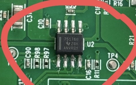
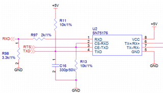
Using SN75176BDR for RS485 communication, as shown in the figure below, the screen printing of the two products is different. The products marked in red circles will affect the burning program (causing poor burning). Could you please help confirm if there have been any changes to the two types of silk screen printing? What are the differences?

Note: The burning signals rxd, txd, and chip pin 1.4 are on the same network.

  • PCN# 20210811000.1 introduced a new die with different characteristics, but the guaranteed datasheet limits have not changed.

    How many termination resistors, with what values, and other components are connected to the bus? Please show a schematic.

    I do not know anything about your burning program. Can you show an oscilloscope trace of the RS-485 bus signals and the corresponding R or D signal, where it goes wrong?

  • Hi Reed,

    Can you please clarify what you mean by burning? Is the device not operating correctly?

    I am going to check those devices internally in case one of them might be a counterfeit device.

    Regards,

    Ethan

  • Under 5V power supply, the output voltage of PIN1 of the circled IC is about 5V, and when it is replaced by 75176 on the right side, the output voltage of PIN1 is about 3.6V. Is the internal resistance changing?

  • Hello Reed and Shitong,

    • Can you please send a schematic of the system?
    • Is the 5V on pin 1 (R pin) a problem for your design? The circled device might be a newer revision. It is possible the drive strength is greater than older versions.
    • For the device on the right (not with the red circle), I cannot make out the bottom line of characters. I am making out "A3_TG4" but that middle character I cannot read. Could you provide this?

    Thanks,

    Ethan

  • Hello Ethan

    • Can you please send a schematic of the system?   

                 see image below

    • Is the 5V on pin 1 (R pin) a problem for your design? The circled device might be a newer revision. It is possible the drive strength is greater than older versions.

                 U2 power supply is 5V, I think the RXD output level of IC should be 5V, the actual test is 3.6V, the specification book display page is 3.6V, right.                   But the red circle IC, the output voltage is not 3.6V directly is 5V, it should be you said that the output capacity is strong, is it also understood that               the internal impedance is also reduced?

    • For the device on the right (not with the red circle), I cannot make out the bottom line of characters. I am making out "A3_TG4" but that middle character I cannot read. Could you provide this?

                 A3VTG4

    Thanks

  • The typical output voltage at the R pin indeed is higher with the new die.

    The schematic shows a voltage divider that results in about 3.3 V. Does it not work?

  • Hi Shitong,

    Thank you for sending that schematic and responses. I see the voltage divider is placed on the RXD line. Voltage dividers should not be used here. If you are worried about the downstream IC voltage level, a level translator is the safest solution. It will cost a tiny bit more but it will guarantee a stable voltage. Another alternative is a 5V input tolerant Schmidt trigger buffer that is tied to an external 3.3V. 

    Even though both devices output different voltages, both are above the minimum requirement of 2.7V and will operate correctly. The graphs you are referencing are only representative of one particular device and should not be taken as exact guarantees (the electrical characteristics table should be used here).

    Regards,

    Ethan

  • It is working, but because the RXD pin output of the 75176 is 3.6V, the voltage is low after passing through the post-stage divider resistance.

  • Thank you for your reply