Part Number: TCAN4551-Q1
Other Parts Discussed in Thread: TCAN4550
Tool/software:
Hello -
I understand the UVLO startup requirements of the TCAN455x (>5.9V worst case to assure proper startup). Also, understand that you can 'bypass' VSUP by applying ~5.2V or greater to the VCCout terminal on the TCAN4550.
A couple related questions:
1) Can you also bypass the LDO by applying 5.2V or greater to the VCCfltr terminal on the TCAN 4551? And that way the CAN bus power will be derived from that terminal rather than VSUP?
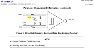
2) Before Vio is applied, is this the proper figure to use for Isup? ~25-42uA?

3) Assuming Vio is applied, SPI active, and CAN bus with ~55 ohm loading, VSUP = 24V, VCCout/VCCfltr applied with external 5.2V, can you help us to estimate Isup? I don't see a figure or way to calculate that.
Thank you & Happy Thanksgiving,
Leon