This thread has been locked.

If you have a related question, please click the "Ask a related question" button in the top right corner. The newly created question will be automatically linked to this question.

TMDS181: TMDS181: Didn't pass the HDMI sink compliance test

Part Number: TMDS181

Dear TI-team,
our custom hardware (TMDS181 + AMD FPGA) comes with an HDMI2.0 receiver interface. We are actually ready for series production, but we didn't passed the HDMI sink compliance test. The external test house IST, reported the following issues:

  • 1. TID8-7 = FAIL
    Verified ID8-7 fail item: The DUT does not display an image.


  • TID8-5 = FAIL
    The DUT is unable to display an image under the following test conditions:


  • TID8-8 & HF2-4 = FAIL
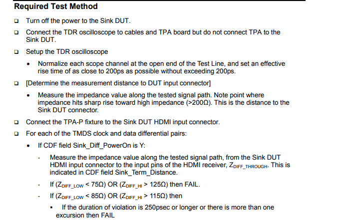
    The Impedance test items TID8-8 & HF2-4 show a Fail in the red-boxed sections(The violation lasted for more than 250 ps). The CTS explanation is as follows:

    Impedance_TID8-8:

    CLK


    The data lanes look very similar as the picture above.
    The same for the HF2-4
    .

What we have already checked:

Anotation:
Since we mixed up TMDS lanes and polarity on PCB, we swapped the lanes and polarity inside the TMDS181, with the drawback, that we can only use the auto-cross-over feature between redriver and retimer. So we decided to let the TMDS run always in retimer only mode...

Dear support team, please can you give us some information how we can pass the compliance test?
We can also send you further design information, but not here in the public forum...

Best regards
STG
 

  • STG

    For TID8-7 (Jitter Tolerance Test)

    Since TMDS181 is in the re-timer mode, they can try the following. They can also leave TMDS181 PLL in its default and see if they can use the FPGA PLL to track and filter out the jitter.

    • Force PLL to lock without changing the PLL loop bandwidth
      • Write 0x01 to register 0xFF. To select Page 1
      • Write 0x23 to register 0x00. To set A_LOCK_OVR
      • Write 0x00 to register 0xFF. To select Page 0
    • Change TMDS181 PLL Loop BW without forcing PLL to lock, and see if it helps to track and filter out the jitter
      • <aardvark>
      • <configure i2c="1" spi="1" gpio="0" tpower="1" pullups="0"/>
      • <i2c_bitrate khz="100"/>
      •  <i2c_write addr="0x5e" count="1" radix="16">09 06</i2c_write> <sleep ms="10"/>   -> Set lane and polarity swap, disable automatically power down base on HDP_SNK
      •  <i2c_write addr="0x5e" count="1" radix="16">FF 01</i2c_write> <sleep ms="10"/> -> Select Page 1 registers
      •  <i2c_write addr="0x5e" count="1" radix="16">01 01</i2c_write> <sleep ms="10"/> -> Charge pump enable. PLL mode, used with the HDMI
      •  <i2c_write addr="0x5e" count="1" radix="16">02 3F</i2c_write> <sleep ms="10"/>  -> Charge pump current control. 7F max charge pump current setting, may need to sweep the value
      •  <i2c_write addr="0x5e" count="1" radix="16">00 03</i2c_write> <sleep ms="10"/> -> Bit 0 -> Enable PLL and Bit 1 -> Enable bandgap
      •  <i2c_write addr="0x5e" count="1" radix="16">0B 33</i2c_write> <sleep ms="10"/> -> Bit [1:0] Loop filter resistance, try setting to 30h and 31h
      •  <i2c_write addr="0x5e" count="1" radix="16">A1 02</i2c_write> <sleep ms="10"/> -> Bit 1 -> Override control for Page 1 register 0x0B, 0x0C, and 0x0D. The register 0x0B write will take effect
      •  <i2c_write addr="0x5e" count="1" radix="16">A4 03</i2c_write> <sleep ms="10"/> -> Bit 1 -> Page 1 Register 0x01 override control. Bit 0 -> Page 1 Register 0x00 override control
      •  <i2c_write addr="0x5e" count="1" radix="16">FF 00</i2c_write> <sleep ms="10"/> -> Select Page 0 registers
      •  </aardvark>

    For (150mV Swing Test),

    • The TMDS181 minimum peak-to-peak input differential voltage is 75mVpp. So with 150mV Swing Test, I would expect TMDS181 to see valid data since differential swing of 150mV is above the TMDS181 minimum input voltage. Do they have the TMDS181 SIG_EN enabled or disabled? If SIG_EN is enabled, I would disable it by pulling SIG_EN low and see if we can get the test to pass. Please also ask the testing house to check their calibration and make sure the differential swing is 150mV at TP2. 

    For TID8-8 & HF2-4 (Impedance Test)

    • They can use an ESD with a lower line capacitance to see if the duration below 85ohm will be shorten to lesser than 250ps. We will also need to see their layout to see if other passive components are contributing to the differential impedance < 85ohm. Do they have a passive TDR measurement on their HDMI input with the bare board?

    Thanks

    David

  • Hello David,
    please see my comments and questions below:

    • Force PLL to lock without changing the PLL loop bandwidth
      • Write 0x01 to register 0xFF. To select Page 1
      • Write 0x23 to register 0x00. To set A_LOCK_OVR
      • Write 0x00 to register 0xFF. To select Page 0

    Why shall I overwrite the lock of the PLL? Does it enable the TMDS outputs on the TMDS181?
    At the moment, I do not understand the reason, why I should overwrite the PLL lock signal?
    Please can you explain the reasons behind this action?

    Second question, when shall I overwrite the PLL lock register? 
    I have no indicator which tells me when I shall override the PLL lock register-
    When the receiver does not detect any input timing, I also do not get any timing detect interrupts...
    Seems to be not practicable...

    • Change TMDS181 PLL Loop BW without forcing PLL to lock, and see if it helps to track and filter out the jitter
      • <aardvark>
      • <configure i2c="1" spi="1" gpio="0" tpower="1" pullups="0"/>
      • <i2c_bitrate khz="100"/>
      •  <i2c_write addr="0x5e" count="1" radix="16">09 06</i2c_write> <sleep ms="10"/>   -> Set lane and polarity swap, disable automatically power down base on HDP_SNK
      •  <i2c_write addr="0x5e" count="1" radix="16">FF 01</i2c_write> <sleep ms="10"/> -> Select Page 1 registers
      •  <i2c_write addr="0x5e" count="1" radix="16">01 01</i2c_write> <sleep ms="10"/> -> Charge pump enable. PLL mode, used with the HDMI
      •  <i2c_write addr="0x5e" count="1" radix="16">02 3F</i2c_write> <sleep ms="10"/>  -> Charge pump current control. 7F max charge pump current setting, may need to sweep the value
      •  <i2c_write addr="0x5e" count="1" radix="16">00 03</i2c_write> <sleep ms="10"/> -> Bit 0 -> Enable PLL and Bit 1 -> Enable bandgap
      •  <i2c_write addr="0x5e" count="1" radix="16">0B 33</i2c_write> <sleep ms="10"/> -> Bit [1:0] Loop filter resistance, try setting to 30h and 31h
      •  <i2c_write addr="0x5e" count="1" radix="16">A1 02</i2c_write> <sleep ms="10"/> -> Bit 1 -> Override control for Page 1 register 0x0B, 0x0C, and 0x0D. The register 0x0B write will take effect
      •  <i2c_write addr="0x5e" count="1" radix="16">A4 03</i2c_write> <sleep ms="10"/> -> Bit 1 -> Page 1 Register 0x01 override control. Bit 0 -> Page 1 Register 0x00 override control
      •  <i2c_write addr="0x5e" count="1" radix="16">FF 00</i2c_write> <sleep ms="10"/> -> Select Page 0 registers
      •  </aardvark>

    Can I use this programming routine for every input timing?
    If not, I have the same issue as before. How do I detect such a situation?

    For (150mV Swing Test),

    • The TMDS181 minimum peak-to-peak input differential voltage is 75mVpp. So with 150mV Swing Test, I would expect TMDS181 to see valid data since differential swing of 150mV is above the TMDS181 minimum input voltage. Do they have the TMDS181 SIG_EN enabled or disabled? If SIG_EN is enabled, I would disable it by pulling SIG_EN low and see if we can get the test to pass. Please also ask the testing house to check their calibration and make sure the differential swing is 150mV at TP2. 

    Do you want to say that the signal detector has problems to detect signals with a diff. swing of 150mVpp, or why should I disable the signal detector?

    By the way, in our design, the TMDS181 will be completely I2C-controlled by the CPU inside the FPGA. We didn't touched bit 4 in the MISC CONTROL register at offset 0x09. So I can tell you, that SIG_EN is low, and the Signal Detector is not used.

    Regarding the second part, asking the test house if they have calibrated their setup, is something I can do. But I think they do not do this test the first time...

    For TID8-8 & HF2-4 (Impedance Test)

    • They can use an ESD with a lower line capacitance to see if the duration below 85ohm will be shorten to lesser than 250ps. We will also need to see their layout to see if other passive components are contributing to the differential impedance < 85ohm. Do they have a passive TDR measurement on their HDMI input with the bare board?

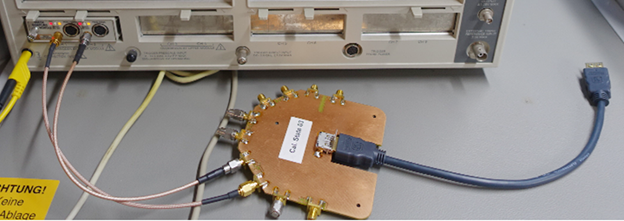
    We have made TDR measurements with and without ESD safety diodes. Below you can see the measurement setup, the top-view part of the PCB with the HDMI-connector, the ESD safety Diodes and the TMDS181, as well as the measurement results, with diodes in (pink line R2) and diodes out (blue line R1). 

    When you compare the pink and blue lines, you can see that there is no difference in the impedance till the position of the ESD diodes. The red line is the position of the HDMI connector, while the line with the red arrow is the position where the ESD diodes will be located. I assume that the second drop down to below 80 Ohm on the pink line, will be the TMDS181 device. 

    When we remove the ESD diodes, we have the hope, that the drop below 85Ohm will not be longer than 250ps, which is in our measurement the case. But I do not know if IST will get exactly the same measurement results as we did...


    Regards
    Steffen


  • Steffen

    For TID8-7 (Jitter Tolerance Test)

    The TMDS181 is designed to be a re-driver when data rates < 1Gbps. As a re-driver, the CDR and PLL are turned off and TMDS181 does not provide any jitter cleaning function, so the jitter will pass onto the FPGA. But since they are using TMDS181 in full retimer mode, the TMDS181 PLL is enabled and having trouble locking at low frequencies. But if PLL is not locked, then TMDS181 will not be in the re-timer mode. They can force PLL to lock or change the PLL BW to see if it will help the PLL to lock, both solutions can be used for all data rates.

    For (150mV Swing Test)

    Can you please share the e2e link which discussed this failure? The e2e link in the previous thread still refers to TID8-7. I am not implying that there is an issue with TMDS181 Signal Detector. When SIG_EN is enabled, the TMDS looks for a valid TMDS clock signal input. The device is fully functional when a valid signal is detected. If no valid TMDS clock signal is detected, the device enters standby mode waiting for a valid signal at the clock input. By disabling Signal Detector, this forces TMDS181 to be in active mode always. For this particular test, can they probe the TMDS181 output? Are they seeing TMDS181 outputs any signal?

    For TID8-8 & HF2-4 (Impedance Test)

    Can they ask IST to perform the active TDR without the ESD diode? Below is the active TDR we took on TMDS181, the excursion below the 85ohm is around 45ps.

    Thanks

    David

  • Hello David,
    here are my comments & questions:

    For TID8-7 (Jitter Tolerance Test)

    The TMDS181 is designed to be a re-driver when data rates < 1Gbps. As a re-driver, the CDR and PLL are turned off and TMDS181 does not provide any jitter cleaning function, so the jitter will pass onto the FPGA. But since they are using TMDS181 in full retimer mode, the TMDS181 PLL is enabled and having trouble locking at low frequencies. But if PLL is not locked, then TMDS181 will not be in the re-timer mode. They can force PLL to lock or change the PLL BW to see if it will help the PLL to lock, both solutions can be used for all data rates.

    I'm a bit confused.Well we use the TMDS181 in re-timer only mode across the full pixel clock range (Register 0x0A, DEV_FUNC_MODE set to 11).

    You say, if the TMDS181 PLL does not lock in re-timer mode, the TMDS181 will not be in re-timer mode ?
    In which mode is the TMDS181 working when the PLL does not lock?

    By the way, if jitter is applied, we can see the PLL lock register toggling betwen 0xC3 and some other values.
    So, even if we would override the lock register by writing a 0xC3 to Page1 Register Offset 0x00, I'm pretty sure, that the TMDS181 will itself overwrite this value again, with some other values... 
    Well overwriting this register does not really make sense, if the value which I have programmed to the PLL lock register, will be permanently overwritten by the TMDS181 itself, or am I wrong?

    For (150mV Swing Test)

    Can you please share the e2e link which discussed this failure? The e2e link in the previous thread still refers to TID8-7. I am not implying that there is an issue with TMDS181 Signal Detector. When SIG_EN is enabled, the TMDS looks for a valid TMDS clock signal input. The device is fully functional when a valid signal is detected. If no valid TMDS clock signal is detected, the device enters standby mode waiting for a valid signal at the clock input. By disabling Signal Detector, this forces TMDS181 to be in active mode always. For this particular test, can they probe the TMDS181 output? Are they seeing TMDS181 outputs any signal?

    Sorry, I did a copy paste mistake regarding the link. Here is the link which I mean:

    https://e2e.ti.com/support/interface-group/interface/f/interface-forum/611375/tmds181-tmds181-failed-hf2-1-of-hdmi2-0-compliance-test

    Well, our test house can't do any measurements. The electronic is burden in the Monitor, and they are not able/allowed to open it.
    But I can tell you, that I do not get any timing detection interrupts at the FPGA, which means, that there was either no TMDS clock signal detected at the FPGA, or the swing of the TMDS clock signal was too small to be detected. Unfortuantely I cannot reproduce this issue in our lab, since I do not have the necessary equipment. We saw, that the TMDS181 PLL was able to lock in this situation. But the FPGA requires a minimum differential peak to peak input voltage swing of 250mV. The question is, whether the TMDS181 has enough gain to achieve the minimum voltage swing for the FPGA?
    Well in re-driver mode, the output voltage swing depends directly on the input voltage swing?
    But how is the behavior for the re-timer mode?

    For TID8-8 & HF2-4 (Impedance Test)

    Can they ask IST to perform the active TDR without the ESD diode? Below is the active TDR we took on TMDS181, the excursion below the 85ohm is around 45ps.


    No, this is not possible. We have to send them a new Monitor with a modified electronic input board. Which costs us time and money. Since we have so many issues, we are currently thinking about a redesign with another Re-Driver / Re-Timer chip...
    In parallel we are also in discussion with our FPGA vendor, in order to find a solution for this issue...

    By the way, the TMDS181 datasheet tells me, that input impedance for the differential TMDS signals can range from 85Ohm - 115 Ohm, which are already the first limits, defined in the Compliance Test. Sounds to me a bit risky to use this chip?


    Requirements Compliance Test:

    Best regards
    Steffen

  • Steffen

    Please see my response below.

    For TID8-7 (Jitter Tolerance Test)

    The TMDS181 is designed to be a re-driver when data rates < 1Gbps. As a re-driver, the CDR and PLL are turned off and TMDS181 does not provide any jitter cleaning function, so the jitter will pass onto the FPGA. But since they are using TMDS181 in full retimer mode, the TMDS181 PLL is enabled and having trouble locking at low frequencies. But if PLL is not locked, then TMDS181 will not be in the re-timer mode. They can force PLL to lock or change the PLL BW to see if it will help the PLL to lock, both solutions can be used for all data rates.

    I'm a bit confused.Well we use the TMDS181 in re-timer only mode across the full pixel clock range (Register 0x0A, DEV_FUNC_MODE set to 11).

    You say, if the TMDS181 PLL does not lock in re-timer mode, the TMDS181 will not be in re-timer mode ?
    In which mode is the TMDS181 working when the PLL does not lock?

    By the way, if jitter is applied, we can see the PLL lock register toggling betwen 0xC3 and some other values.
    So, even if we would override the lock register by writing a 0xC3 to Page1 Register Offset 0x00, I'm pretty sure, that the TMDS181 will itself overwrite this value again, with some other values... 
    Well overwriting this register does not really make sense, if the value which I have programmed to the PLL lock register, will be permanently overwritten by the TMDS181 itself, or am I wrong?

    If the TMDS181 is configured for retimer mode, the PLL needs to be locked to enable the retimer function. If the PLL is not locked, then TMDS181 will be in the redriver mode.

    When overwriting the register, the write will override the lock detect and force the lock bit to be always true, so TMDS181 will not able to change it.

    For (150mV Swing Test)

    Can you please share the e2e link which discussed this failure? The e2e link in the previous thread still refers to TID8-7. I am not implying that there is an issue with TMDS181 Signal Detector. When SIG_EN is enabled, the TMDS looks for a valid TMDS clock signal input. The device is fully functional when a valid signal is detected. If no valid TMDS clock signal is detected, the device enters standby mode waiting for a valid signal at the clock input. By disabling Signal Detector, this forces TMDS181 to be in active mode always. For this particular test, can they probe the TMDS181 output? Are they seeing TMDS181 outputs any signal?

    Sorry, I did a copy paste mistake regarding the link. Here is the link which I mean:

    https://e2e.ti.com/support/interface-group/interface/f/interface-forum/611375/tmds181-tmds181-failed-hf2-1-of-hdmi2-0-compliance-test

    Well, our test house can't do any measurements. The electronic is burden in the Monitor, and they are not able/allowed to open it.
    But I can tell you, that I do not get any timing detection interrupts at the FPGA, which means, that there was either no TMDS clock signal detected at the FPGA, or the swing of the TMDS clock signal was too small to be detected. Unfortuantely I cannot reproduce this issue in our lab, since I do not have the necessary equipment. We saw, that the TMDS181 PLL was able to lock in this situation. But the FPGA requires a minimum differential peak to peak input voltage swing of 250mV. The question is, whether the TMDS181 has enough gain to achieve the minimum voltage swing for the FPGA?
    Well in re-driver mode, the output voltage swing depends directly on the input voltage swing?

    But how is the behavior for the re-timer mode?

    Thanks for sharing the link, this goes along with my line of thinking as well. With TMDS181 peak to peak input differential voltage at minimum of 75mV, I would expect TMDS181 to see the 150mV input signal unless there is a large drop of signal amplitude to be below 75mV. For TMDS181 output signal amplitude adjustment, you can tune the VSADJ resistor. Reducing the VSADJ resistance will increase the output signal amplitude. The VSADJ adjustment applies to both re-timer and re-driver mode.

    For TID8-8 & HF2-4 (Impedance Test)

    Can they ask IST to perform the active TDR without the ESD diode? Below is the active TDR we took on TMDS181, the excursion below the 85ohm is around 45ps.


    No, this is not possible. We have to send them a new Monitor with a modified electronic input board. Which costs us time and money. Since we have so many issues, we are currently thinking about a redesign with another Re-Driver / Re-Timer chip...
    In parallel we are also in discussion with our FPGA vendor, in order to find a solution for this issue...

    By the way, the TMDS181 datasheet tells me, that input impedance for the differential TMDS signals can range from 85Ohm - 115 Ohm, which are already the first limits, defined in the Compliance Test. Sounds to me a bit risky to use this chip?


    Requirements Compliance Test:

    The 85ohm is the minimum input differential termination impedance, majority of device will have the typical 100ohm differential input impedance.

    Thanks

    David