This thread has been locked.

If you have a related question, please click the "Ask a related question" button in the top right corner. The newly created question will be automatically linked to this question.

Rugged LVDS Driver/Receiver again

Other Parts Discussed in Thread: DS90C032, DS90C031, DS90C3202, DS90C3201, SN65LVDS348, DS91M040

Hello,

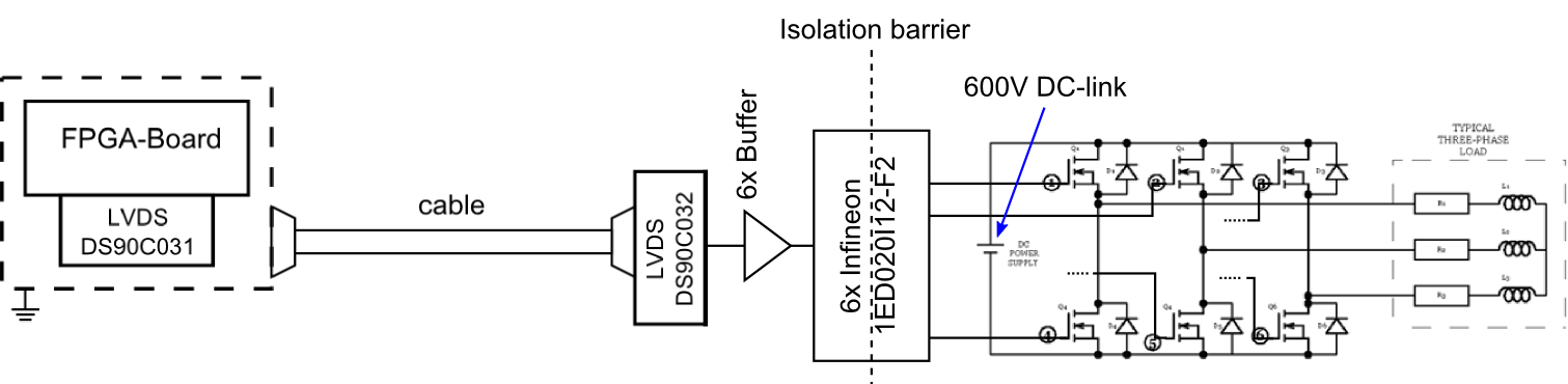
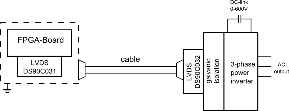
we are using the DS90C031 / DS90C032 Driver/Receiver to drive a three phase power inverter (600V@50A ~30kW) from a custom FPGA-Board. The cable is shielded, twisted pair and about 2m long. The power inverter uses SiC MOSFETs which are switching very fast (~100ns), so we have a high dV/dt. Thats why we have much noise on the cable that causes the Receivers to fail and sometimes they get destroyed. We added some common mode chokes at the inputs of the receivers. Now we got some more room but at 600V DC-link voltage the noise increases and the failures are back again. So what could be done that the receivers don't fail any more? Use another diff. signaling standard (e.g. PECL)? Other drivers/receivers with more common mode voltage tolerance?

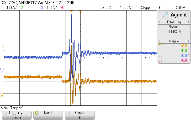
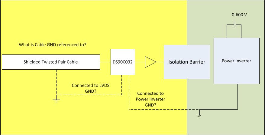
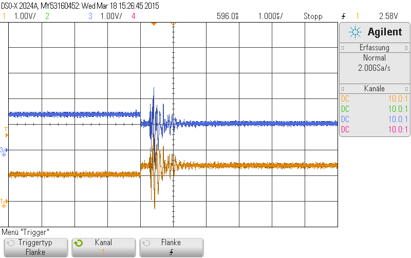
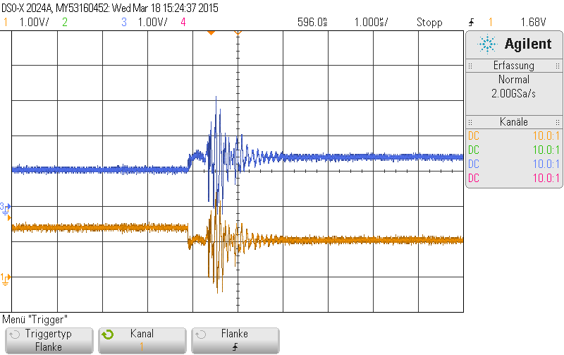
I added an overview of the setup and some oscillographs of the p-n LVDS wire. The high common mode noise could be seen on the plots which gets higher with increased DC-link voltage. I already found a thread that discusses this topic but unfortunately its closed without a visible result (http://e2e.ti.com/support/interface/high_speed_interface/f/138/t/402489).

LVDS p-n wire @ 100V DC-link voltage

LVDS p-n wire @ 200V DC-link voltage

LVDS p-n wire @ 300V DC-link voltage

  • Hi Julian,

    Thanks for the background information and the additional waveforms. I presume these waveforms have been taken right at the input of the DS90C3202?

    This type of common mode noise is dangerously beyond the allowable Vcm range specified by the DS90C3202 receiver (0.2 Vmin to 3.2 Vmax). particularly in that last case when power inverter DC input = 300V causes the common mode voltage to swing above 3.3V and below 0 V.

    Typically LVDS is a good signaling topology in a noisy environment, because compared to CML and PECL, it has the largest allowable common mode range and it operates at the lowest power due to low differential signal amplitude. 

    I agree that there is some isolation issue, since this noise appears to be affected by the DC link voltage for the power inverter. I'd suggest a few ideas:

    1. Try cutting or disconnecting the DS90C3202 from the galvanic isolator and measure the LVDS input as you crank up the DC link voltage. We just want to confirm that it is the power inverter somehow feeding parasitic voltage back to the DS90C3202 LVDS input that is causing this, and not the FPGA or DS90C3201 transmitter.

    2. What is the galvanic isolator you are using? Is it an optocoupler? My next idea was to try adding additional isolation components like an optocoupler to see if this improves the receiver's resilience to common mode noise.

    3. What kind of decoupling do you have on the VDD supply voltage? It is possible that without enough decoupling, your supply voltage level is unstable and contributing to the common mode noise somehow when the DC link voltage is changed.

    Thanks,

    Michael

  • Hello Michael,

    thanks for your reply and your suggestions. Unfortunately i cant disconnect the DS90C3202 from the galvanic isolation because this drives the MOSFETs and thats what causes the EMI. When is stop driving the MOSFETs the common mode noise disappears. The same thing when i reduce the DC-link voltage. So in my opinion the common mode noise is caused by the switching transients of the power MOSFETs and injected into the cable over the air..? I added a more detailed schematic of my setup.

    The Infineon 1ED020I12 driver uses inductive coupling for galvanic isolation. I dont think that noise from high voltage secondary side is coupled to primary side.

    We used 100nF bypass capacitors very close to the driver/receiver for decoupling but it could be improved by adding some ferrits. Thats a good idea. Do you think using another driver/receiver with enhanced common mode voltage range (e.g. SN65LVDS348) could improve the situation? Is PECL more resistant against common mode noise than LVDS due to increased voltage difference level? Power consumption doesnt matter at all.

  • Hi Julian,

    I think if this issue is causing the part to fail, it is not as much a common mode voltage range issue as it may be that the device is being thrown out of its absolute maximum rating. I do not think moving to another device with enhanced common mode voltage range will necessarily improve the issue. Likewise, since this is something you are seeing on the common mode, picking a signal topology with a larger differential voltage level may not resolve your issue either.

    From the waveforms you have provided, it appears that the large voltage spike is a transient that occurs when a DC-link voltage is applied. Is that correct? What appears that may be a problem is that the isolation barrier is somehow not able to provide enough isolation and may actually be causing a shift in the GND reference that is destroying the internal ESD structure of the DS90C032 due to an excess amount of current caused by disturbances from the inverter.

    Can you try out a few other things so we may be able to dig into where the root of the problem is? I have made a diagram below of some questions we have:

    1. Can you probe both the DS90C032 VCC and GND when this spike is happening? I wonder if the spike is occurring due to a shift in the reference levels.

    2. According to the board design you have, is the DS90C032 GND reference separate from the inverter GND reference? I am assuming that they are, since you have an isolation barrier, but if you could explain where each device is referencing GND, it may help us see if there's a possible current path to flow unintentionally into the LVDS portion of your design.

    3. What is the cable shield referenced to? I presume that it shares its GND with the LVDS receiver only. Is that correct?

    4. Do you have a schematic or layout that you can share for this design?

    Thanks,

    Michael

  • Julian,

    I agree higher input common mode range would help.  Also lowering the common mode impedance would help.

    Using a 50 ohm x 2 input termination for each LVDS Rx and adding a large common mode cap would damp the common mode coupling you are seeing.

    Adding ESD diodes at the LVDS input in conjuction with higher range common mode devices like the DS91M040 or SN65LVDS348 would also help to create another low impedance path once the signal voltage went outside the GND to VDD range.

    Lee

  • Thanks a lot! The splitted termination resistor is another great idea. I will give it a try...