This thread has been locked.

If you have a related question, please click the "Ask a related question" button in the top right corner. The newly created question will be automatically linked to this question.

Connection of DS90UB913A-Q1 & DS90UB914A-Q1 for HD Camera

Other Parts Discussed in Thread: DS90UB914A-Q1, DS90UB913A-Q1, DS90UB913A-CXEVM, DS90UB914A-CXEVM

Hi,

We are now developing camera module for automotive for HD grade with LVDS solution.

We have done the camera module with image sensor and working fine. 

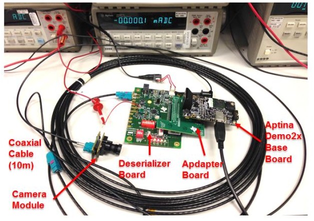
When connect the image sensor module + DS90UB913A-Q1 and using Power Over Coaxial, and link to DS90UB914A-Q1 + SoC board, the image sensor board cannot view and control.

Below is the detail:-

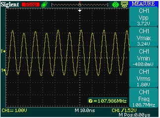
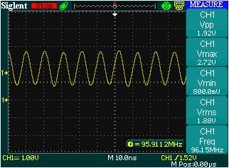
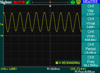
1) As DS90UB913A-Q1 are connect to image sensor module, it was set to have Pixel Clock input to Serializer.

2) The PASS LED and LOCK LED able to turn on when both DS90UB913A & 914A are connected through PoC.

3) After checking, there is no Pixel clock are output from image sensor to DS90UB913A-Q1.

4) My question is:-

   a) Does the LVDS for Ser and Der will only be start to function (Connection be establish) and transfer the data when the Pixel Clock are input to the Serializer?

   b) The I2C control signal cannot be transfer from Der to Ser or vice versa if there is no Pixel clock input to the Serializer? 

Hope Someone can help me on this.

  • Hello Kah Joo Lee,

    If no pixel clock input is being sent into the 913A from the imager, then this is an issue with the imager. If no pixel clock input is provided from the imager (in PLCK mode or external oscillator mode) then the parallel imager data being sent to the 913A will not be synchronized and the system will not work.

    a) Does the LVDS for Ser and Der will only be start to function (Connection be establish) and transfer the data when the Pixel Clock are input to the Serializer?


    Answer: No, the Serializer and deserializer will function and send data over LVDS without the imager or SoC connected. This can be seen when a 913A EVM is hooked up by a cable to the 914A EVM - you will see LOCK and PASS go HIGH when a connection is established even without a pixel clock input from the imager. The reason for this is because there is an internal PLL that is generated inside the 913A chip - when no PCLK input is detected, the chip switches over to this internal oscillator which is ~ 50 MHz by default ( and can be changed through a register). Probing the PCLK output on the 914A IC will show this signal.


    b) The I2C control signal cannot be transfer from Der to Ser or vice versa if there is no Pixel clock input to the Serializer?

    Answer: The I2C control signals are independent of the pixel clock from deserializer to serializer - these signals are transferred over the backchannel. The I2C control signals are transferred within the forward channel payload from serializer to deserializer - even if no pixel clock input exists, I2C data will still be transferred from Ser to Des because the device will switch over to it's internally generated clock as mentioned above.

    Regards,

    Sean

  • Hi Sean,

    Thanks for your replied.

    Current we are making the working prototype base on TI Eval board as the board setup as reference from TI.

    We have the Aptina demo board as well and we have the camera module using Aptina AR0132 + AP0100AT similar to TI design.

    I've manage to powered and connect the LVDS Ser & Der and the PASS & LOCK was high with LED turn on.

    However, when I connect the camera module + Serializer and connect through PoC to Deserializer+Aptina Demo board, the DevWare(Aptina image sensor Software) the software can't detect the Image sensor.

    For the Image sensor module, the I2C are slave and and the DevWare Software (Aptina Demo Board) are Master of the I2C. At the DevWare Software start up, it will check for the image sensor by sending the I2C.

    From your explanation, the I2C can be transfer only from Ser -> Der when there is no Pixel Clock?

    So I2C cannot transfer from Der -> Ser to control the image sensor?

    Can I said that, I need to pre-program the Image Sensor so that it can output the parallel data + Pixel Clock to Ser, so that the I2C can be transfer in bi-directional?

    By the way, do your side have the setting and share to us how the demo set for (Aptina™ Automotive Camera Module) so that it can be view in Aptina's DevWare?

    Thanks for your great support.

  • Hello Kah Jo Lee,

    The I2C can indeed transfer data from DES --> SER to control the image sensor according to your setup above. It does not need the external PCLK applied from the Aptina image sensor to transfer I2C data over the backchannel (from DES --> SER). With the setup you have above, LOCK and PASS being HIGH is a good sign that everything is working properly between the 913A and 914A communication link.

    The problem you are seeing is most likely an issue with the Aptina Demo2x base board. In order to obtain the software and settings to program the Aptina image sensor, you will need to contact Aptina directly.


    -Sean

  • HI Sean,

    1) I've set the image camera to have initialize data and output the picture data out from image sensor and able transfer fromTI Eval board of Ser -> Der output. However I've notice the Pixel Clock swing was not same as Pixel clock at Ser input side as picture below.

    Pixel Clock input from image sensor to Ser:-

    Output of Pixel Clock from Der without connect to any circuit from TI Eval board:-

    What is the problem at the Der Pixel clock output?

    How we can overcome this?

    2) We need to have I2C to be communicate from Host to image sensor through Der -> Ser. What setting need to be done instead to have bi-direction I2C data transfer?

    Thanks.

  • Hello Kah Joo Lee,

    1) If you do not connect the image sensor, what is the output PCLK waveform and frequency that you see on the Der? Please post this. Also, where are you probing for the pixel clock input ? The best place to probe is the PCLK header pins which are soldered onto the left-side of the 913A EVM. Finally, are you probing the Der PCLK output on the header pins located on the right-side of the 914A EVM?

    2) For configuring the registers to send I2C data through Der --> Ser, first you must set one of the Slave ID[x] (x = 0 through 7) registers which begin at address 0x08 on the 914A. This Slave ID[x] register should be written with the I2C device ID value of your remote slave (i.e. the image sensor). As long as you do not have duplicate devices with the same I2C address as your serializer or image sensor then you should not have to configure the slave alias registers on the 914A and can address the image sensor or the 913A with their respective addresses.

    -Sean
  • Hi Sean,

    1) I've capture the PCLK from Eval board of 914A at the JP1 header. For the last post, I also probe the signal at the header pin of PCLK on the EVAL board as well. Does the PCLK are correct of signal are not reach 0V as shown?

    2) I'll try a way to configure the I2C of the 914A.

    Thanks.

  • Hello,

    The PCLK image above from the 914A should be correct. There will be a small amount of DC offset on PCLK as verified in the laboratory.

    -Sean

  • Hi Sean Thornton,
    In the Aptina Camera module reference design (www.ti.com/.../TIDA-00098) uses a DS90UB913A-CXEVM & DS90UB914A-CXEVM to interface with Aptina Demo2X board. In the document it is mentioned that a "Modified Adaptor board" is used to interface with Demo2x board. I could not find much information in the link.
    Do you have the schematics or signal details associated with Modified Apator board
  • Hello Sean,
    I've set the image camera to have initialize data and output the picture data out from image sensor , but when I connected the picture data to 913A, I can't detect the picture data in ROUT Pin on 914A,but only can detect the PCLK Pin on 914A. Maybe the transfer fromTI Eval board of Ser -> Der output is unsuccess?what can I do to solve this problem ?
    Looking for your reply! Thank you so much!