


Type-C and PD comes with awesome new functionalities and even more design challenges. The Type-C connector comes in many flavors and the most difficult (Jacob’s Opinion) is the mid-mount SMT connector with EMI ground shielding. Here are a few tips we have used across many of our reference designs and EVMs (Evaluation Modules) that a PCB designer can use to help make routing the connector as easy as possible.
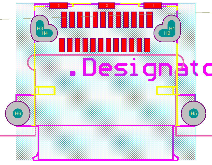
Step 1: Get the latest footprint symbol from your Type-C connector vendor and double check it. And check it again. In the ideal case, working with your board manufacturing partner to verify the footprint and planarity of the connector. When you build for volume, a small percentage of failures will quickly come to haunt you. A test-build could also save money down the road to work out any issues that may come up. Below is the footprint for the connector used on our TPS6598x BoosterPacks.
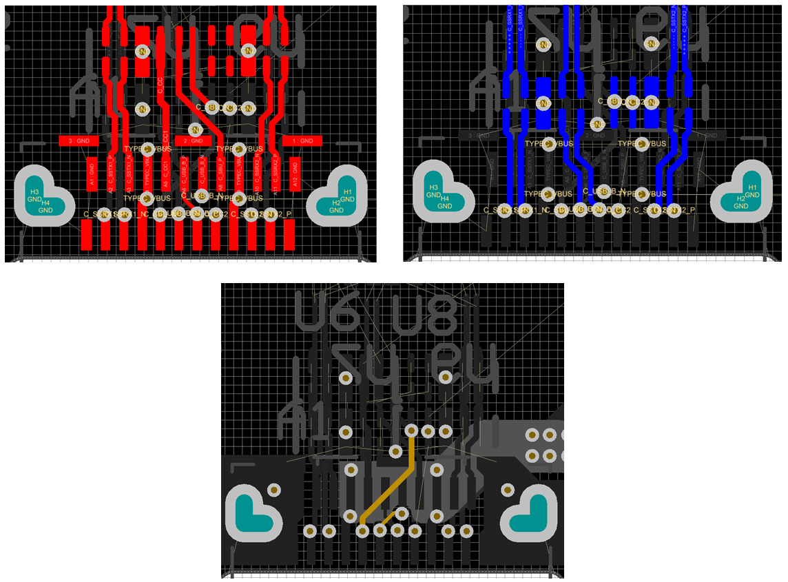
Step 2: Once you found a home for your connector, get started on placing vias. From some previous test builds we have found that it is best to use through-hole 8/16 mil vias (no blind and buried vias). As far as design rules, we are setting our difference net spacing to 3 mil (worst case) and tenting our vias (top/bottom). Make sure the via hole does not hit the pads on the Type-C connector to avoid “via on pad”. Check the via placement on the connector below. This connector shorts the Top/Bottom USB2 pins.

Step 3: Get those SSTX/RX pairs out on the top and bottom layer. Since these are the most crucial signals, make sure they get out cleanly to reduce the amount of “serpent” bends you have to do to match their lengths. Refer to you board’s designs rules for proper differential impedance.
Step 4: The SBU, USB2, and CC1/2 pins are next to be routed. Check out the TPS65982 datasheet for the widths for CC1/2 and refer to you board’s designs rules for proper differential impedance. The
The figure below show the SSTX/RX pairs, USB2, CC1/2, and SBU routing on the top/midlayer/bottom/ layers.
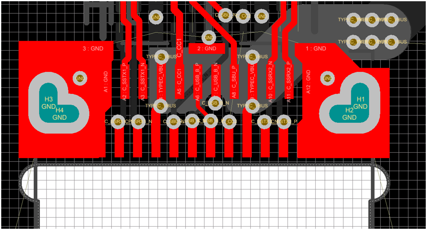
Step 5: Getting 5A to the Type-C connector is a challenge especially when copper is a luxury close to Type-C connector. There are two methods we have used with good results. The first is using a sizable plane on an inner layer to carry the high current. About 125 mill of copper width is needed for 0.5 oz copper to safely carry 5A. The second method is to use the top/bottom layer to carry the bulk of the current (place trace/pours away from data path) and about 65 mils with 0.5 oz copper with platting (0.5 oz) will easily carry 5A. Once the power is close to the connector dedicate two pours on an inner layer to hit the VBUS vias under the connector and use a bank of vias to stitch them to the top/bottom pours.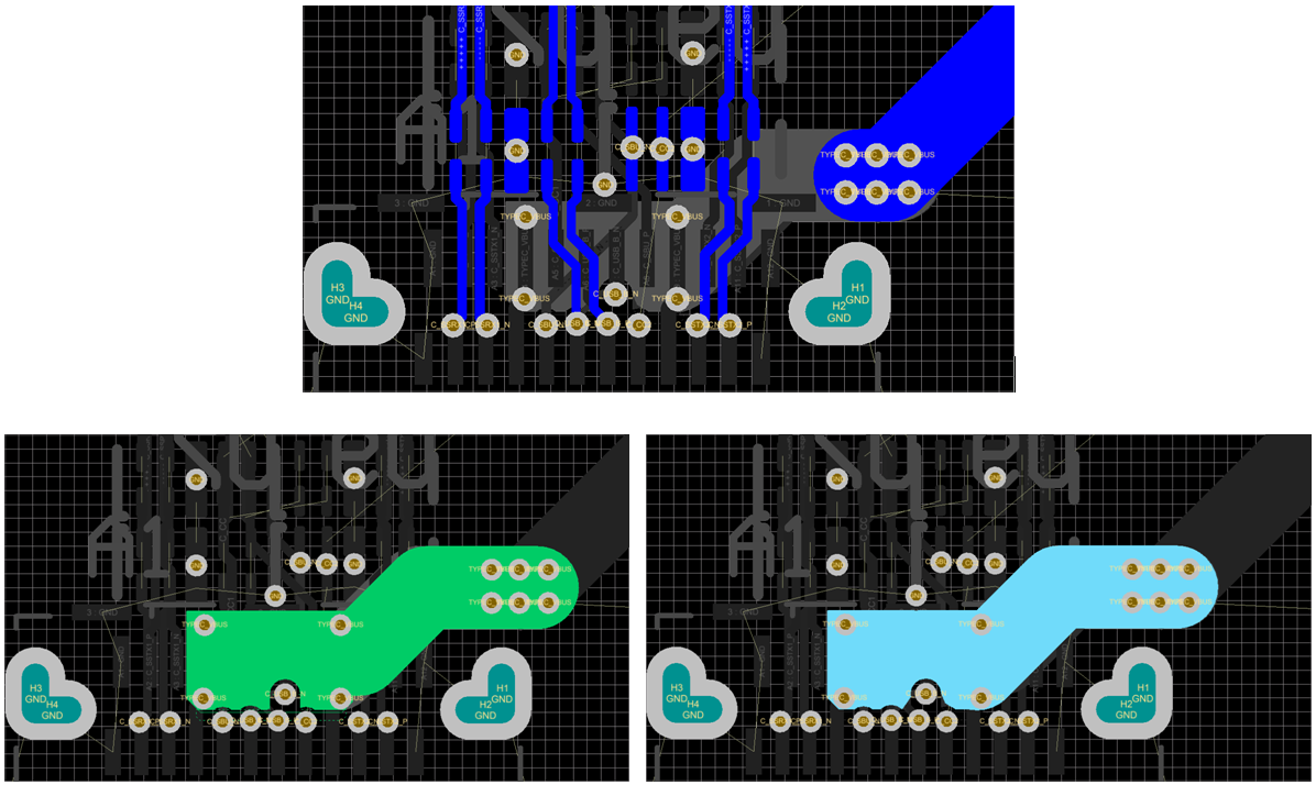
Step 6: GND pours. Fairly straight forward pour on the top layer with a few additional vias. The pour can be expanded to connect the stabilizing through-holes on the front of the connector.
These tips can be applied to other Type-C connectors and should help reduce the amount of time (headaches) when doing layout on a Type-C system. A few other tips are to stack your ESD protection on top and bottom in order to get them as close to the Type-C connector and to align your Type-C and PD devices like the TPS6598x PD controller and HD3SS460 mux to minimize the amount bends. Check out our EVMs and reference designs to see the layout firsthand.
Jacob

