This thread has been locked.

If you have a related question, please click the "Ask a related question" button in the top right corner. The newly created question will be automatically linked to this question.

LMH0041: LVDS Output Verification

Part Number: LMH0041
Other Parts Discussed in Thread: LMH0344,

Hi, all.

I designed HD-SDI DES(Receiver) Board of 2 versions below as below.

But it does not all work well. 

The FPGA(Zed Board) did not recognize the LVDS signal well. 

I would like to know what is wrong.

Please see below details.

V2.0 PCB Top side

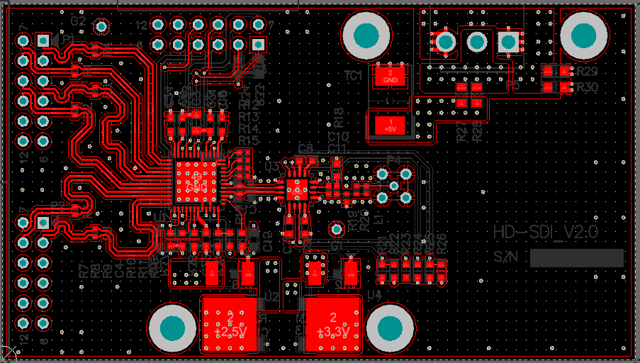
LVDS output trace impedance is 100 ohm (differential) on PCB.

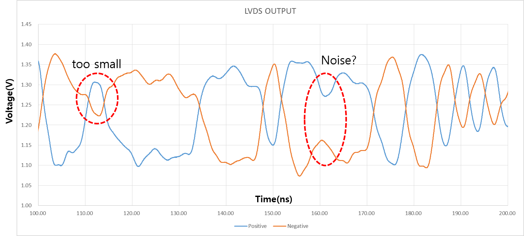
The FPGA did not recognize the LVDS signal. (Zed Board) 

LVDS Data output is too strange as Below . 

Measurement environment

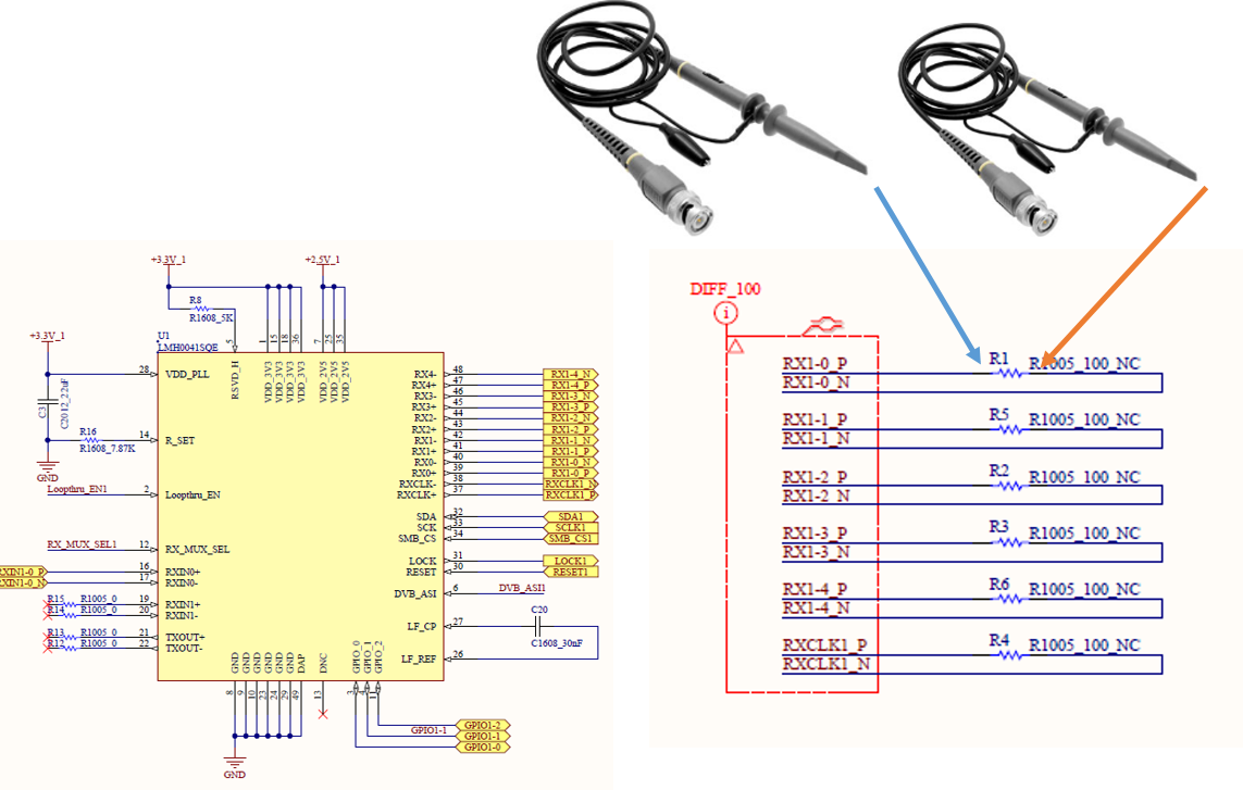
* C20 uses 27nF instead of 30nF.

  • Hi Asher, 

    1). Loopthru_EN pin 2:

    It seems you are not using TXOUT pins(pine # 21 & 22). Please make sure when you are running your test Loopthru_en is disabled.

    2). Could you please put your scope probe on LOCK/ to make sure it is always low when you have signal connected.

    3). What pattern are you using for this evaluation? I noticed 1010.. pattern at the end of your waveform. Do you see a similar issue when you use color bar pattern?

    4). I am assuming if you don’t put scope probe FPGA still has problem decoding incoming video/ Right?

    5). What video rate are you operating at? Do you see similar issue at SD or 270Mbps rate? Please note for 270Mbps operation we need to put DVB_ASI pin high.

    6). Do you see a similar problem if you use a clean 3.3V lab power supply? I am trying to make sure there is not power supply noise since I don’t see much power supply coupling caps.

    7).  Please attach LMH0344 schematic to this case as well.

    I compared LMH0041 internal schematic with your schematic and did not see a difference. I have attached this schematic to this case and you can review as well.SDV DeSerializer EVK Schematics Oct 23 07.pdf

    Regards,,,,, Nasser

  • Thank you for reply.

    HD-SDI_V2.0-SCH.PDF

    I attached my schematic

    1). Loopthru_EN pin 2:

    It seems you are not using TXOUT pins(pine # 21 & 22). Please make sure when you are running your test Loopthru_en is disabled.

     - Loopthru_en is grounded. (Disabled)

    2). Could you please put your scope probe on LOCK/ to make sure it is always low when you have signal connected.

      - It is always low when signal connected. I found a strange point. When signal disconnected, High level of LOCK/ pin is 2.5V. 

    3). What pattern are you using for this evaluation? I noticed 1010.. pattern at the end of your waveform. Do you see a similar issue when you use color bar pattern?

      - I can't using pattern. I just use HD-SDI output of CMOS image sensor board (1.485GHz/1920x1080/30frame). 

    4). I am assuming if you don’t put scope probe FPGA still has problem decoding incoming video/ Right?

      - Right. It still has problem without scope probe. 

    5). What video rate are you operating at? Do you see similar issue at SD or 270Mbps rate? Please note for 270Mbps operation we need to put DVB_ASI pin high.

      - I just use HD-SDI output of CMOS image sensor board (1.485GHz/1920x1080/30frame). 

    6). Do you see a similar problem if you use a clean 3.3V lab power supply? I am trying to make sure there is not power supply noise since I don’t see much power supply coupling caps.

      - I used 5V from power supply. LDO generated 3.3V and 2.5V. I think almost clean power.

    7).  Please attach LMH0344 schematic to this case as well.

    I attached my full schematic.

  • Hi Asher,

    Thanks for the reply.

    Based on your responses, here are some comments:

    1). I checked LMH0344 schematic and did not see a problem.

    2). It would have been a good idea if we can use a regular pattern like color bar but I understand your image sensor may not support this. Please take the output of the image sensor to a regular HD video analyzer just to make sure video goes through with no problem(you may have already done this).

    3). In your response, you had noted LOCK/ when in-active is 2.5V instead of 3.3V level. Please take a look at page 12 of data sheet to make sure we are compliant with power supply DC coupling and more importantly power sequence. Please check to make sure 3.3V or 2.5V is going to the right pins. We need to understand why we see 2.5V instead of 3.3V on LOCK/pin when inactive this. This could tell us why you are seeing this issue.

    Regards,,,,, Nasser

  • Thank you for your details.

    1). I checked LMH0344 schematic and did not see a problem.

      - I think so, too.

    2). It would have been a good idea if we can use a regular pattern like color bar but I understand your image sensor may not support this. Please take the output of the image sensor to a regular HD video analyzer just to make sure video goes through with no problem(you may have already done this).

      - I had a similar test. I used a "HD-SDI to HDMI Convertor" for  image sensor sigmal validation with HDMI display. I checked a image sensor worked well.  

    3). In your response, you had noted LOCK/ when in-active is 2.5V instead of 3.3V level. Please take a look at page 12 of data sheet to make sure we are compliant with power supply DC coupling and more importantly power sequence. Please check to make sure 3.3V or 2.5V is going to the right pins. We need to understand why we see 2.5V instead of 3.3V on LOCK/pin when inactive this. This could tell us why you are seeing this issue.

      - I found the wrong part in my schematic. The parts(2.5V LDO and 3.3V LDO) have been swapped. 

    So I fixed that. And I measure High level of LOCK/. It was 3.3V level. I think it is normal. But LVDS DATA OUTPUT still strange.

    The VDD2V5 pin on LMH0041 applied over voltage(3.3V) during test continuosly. 

    Is there any possibility that abnormal LVDS DATA OUPUT happens due to chip damage?

  • Hi Asher,

    Yes it is possible that device may have gotten damage.

    Please take care of the 3.3V supply first and then check another part. Or i was going to ask if you have seen this problem on more than one board.

    Regards,,nasser
  • Hi Nasser,

    I have seen strange LVDS DATA OUTPUT of LMH0041. 

    There had 2 problems.

    First, Power sources were swapped. (3.3V and 2.5V)

    Second, method of measurement was wrong.

    This time, I used differential probe. (I rent the differential probe for this)

    So, I saw clear waveform. 

    (Actually LMH0041 are not damaged. It just had been wrong method of measurement for LVDS.)

    But I still have a problem. The FPGA of ZED board did not recognize the LVDS signal well, still.

    LVDS signals must be transmit to ZED board(Made by digilent) without distortion. 

    Here is a problem. 

    termination resistor pads are not on ZED board.

    So, I applied termination resistor on my board"HD-SDI Receiver V2.0"

    The termination resistor is much closer to the LMH0041 (transmitter) than the FPGA (receiver).

    It is estimated that this causes signal distortion. what do you think?

    I am trying to figure out how to apply a termination resistor on a ZED board.

  • Hi Asher,

    Agreed termination should be at the end of transmission line. If termination is at the transmitter then trace going to the receiver acts like stub and you could have reflection . However i cannot say this is the root cause of the issue you are seeing. Do you see the same problem at lower data rates? i am thinking perhaps this termination issue could have less effect at lower data rate.

    Regards,,nasser

  • Hi Nasser,

    This resolved my issue. 

    I applied the termination resistor at my ZED board(Avnet).

    After that It was confirmed that the signal was properly transmitted without distortion.
    (It's too difficult that soldering resistor for termination at the VIA and at the pattern of LVDS pair. But I done it.)

    Thank you for your help.  

  • Hi Asher,

    I am glad you got it working and thanks for letting us know.

    Regards,,nasser