This thread has been locked.

If you have a related question, please click the "Ask a related question" button in the top right corner. The newly created question will be automatically linked to this question.

TCA9800: Noise on data and clock lines - SMBUS - multiple clients

Part Number: TCA9800
Other Parts Discussed in Thread: BQ25708, BQ40Z50, TCA9517

This question/note is related to the content here:

http://e2e.ti.com/support/interface/f/138/p/728240/2688842?tisearch=e2e-sitesearch&keymatch=TCA9800#2688842

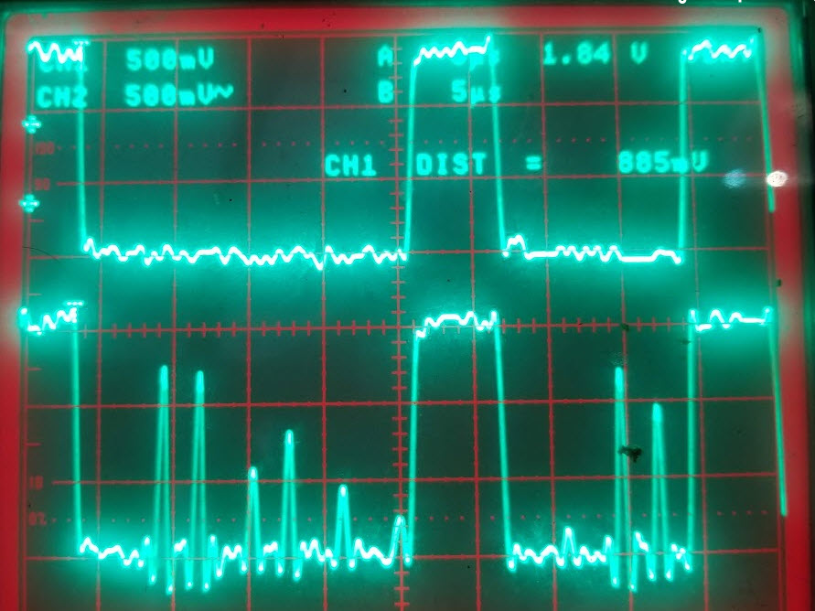
In the problem, the TCA9800 is used to isolate the system CPU (Microchip/Atmel SAMG55) from a "smart battery" pack and our battery charge controller.  The smart battery uses a BQ40z50 battery manager.  Our charge controller is the BQ25708.  The problem occurs when the charge controller turns on and supplies charge to the battery pack.  It exhibits itself with corruption of the data line with sporadic noise at roughly the switching frequency of our charge controller.  Here's a scope presentation:

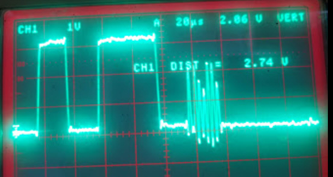
And here's what it looks like in a protocol analyzer:


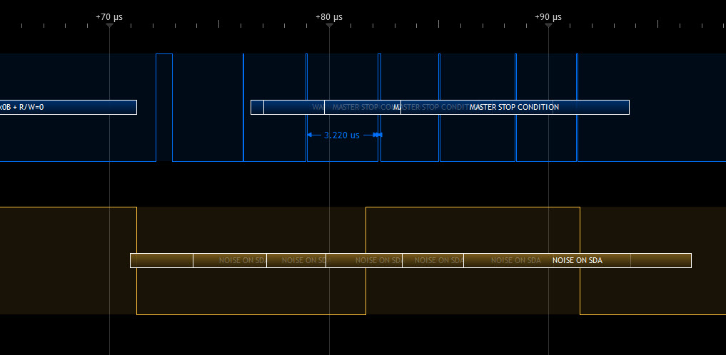
The noise appears to present itself when an ACK is expected.

After a lot of head scratching, it occurred to me that the TCA9800 B side, which is the side that services our charge controller and smart battery pack with data and clock, determines a low based upon how much current it detects is being drawn from an external device.  Given that we have two "client" devices on the SMBUS (the CPU twi/SMBUS is on the A side of the TCA9800) I wondered if the electrical interface of each device SMBUS lines were, when combined, causing the problem.

When we first designed our system, 100 ohm series resistors were used in SMBD and SMBC at the smart battery connector for the purpose of damping any ringing during level transitions.  Could this (low) series resistance be adding just enough resistance that devices on the buss have insufficient ability (perhaps due to RDS ON in their output switching fets) to draw sufficient current from the TCA9800?

When I removed the 100 ohm series resistance, the problem went away entirely.  I have been unable to bring it back (so far)!

Questions:
1. Is my theory sensible?
2. The electrical interfaces of both the BQ40z50  and the BQ25708 are not adequately defined (AFAIK) in the data sheet.  I'm not sure the SMBUS specification deals with current sinking/sourcing ability of the interface, nor whether these are relevant in situations where the buss is shared between (in this case) the devices we are using.
3. What happens when ACK is expected?  It appears it's at this point in the SMBUS signal state that the noise appears.  
4. Since the noise is at the switching frequency of the BQ25708, it seems reasonable to assume this device is our culprit.  Is it?

I suppose this kind of issue could be solved with a more selective interface/DSP on the CPU side... for example, having a minimum clock and data width.  But this doesn't help when the CPU is out of the equation.. which occurs when the battery pack sends charging data on the bus which is picked up by the charge controller and acted upon (the "smart" side of the house).  With a mangled SMBUS, those comms would be ruined, as would any safety features we wish to implement through monitoring for alarms.  Therefore it was imperative to solve this.

Hopefully we did so, but I'd like to hear from TI on this particular scenario.


  • Hey K1mgy,

    "1. Is my theory sensible?"

    "Could this (low) series resistance be adding just enough resistance that devices on the buss have insufficient ability (perhaps due to RDS ON in their output switching fets) to draw sufficient current from the TCA9800?"

    -Yes. This device monitors the current source on B side to see if B side is sourcing or sinking current. B side sinks current when A side drives low (think of a NFET on B side driving low and it sinks the current source). It sources current when A side is high and B side slave/master is NOT driving low. The exception is during an ACK.

    There is a unique situation that occurs in I2C where contention is expected and that is during the 9th clock cycle where you expect an ACK so the master/slave driving SDA will release the bus to get the 'handshake' from the receiver to confirm the message was received. This is a situation where lets say the master is on A side and drove the bus low but then releases the bus to let the slave on B side drive the bus. Now in TCA9800 A side drives low so B side's NFET is turned on and sinking current, B side needs to know to drive A side low during this handoff. The internal logic is if A side is currently low and B side will only redrive a low back to A side when the device sees that it is sourcing current (opposite of it's normal logic). This means that the slave must drive enough current from B side of the device to detect the slave ACKing and send a low back to A side in time.

    Now if you have a series resistor on B side, then the overall current that can be sourced during this event is lower. Essentially the effective resistance is now Rdson of the slave's NFET plus the series resistance. Section 9.4.1.1.2 states the requirement of Rdson of 150 ohms or less to ensure that you source enough current during the contention state to properly send an ACK. By placing a 100 ohm series resistor you have effectively lowered the allowable resistance of the slave's NFET to be 50 ohms or less.

    Now here is the unique thing of this. I believe what is happening is the slave's NFET's Rdson is changing when you are seeing this 'bug' occur. Recall that the NFET is operating in the triode (linear) mode of operation (not saturation) and rdson will change as a function of Ids (higher Ids means lower Rdson). Because you have limited the current going into the NFET by the 100 ohm resistor Ids is lower and thus Rdson of the slave's NFET is now larger when rdson settles and could potentially be higher than the 50 ohm allowance (should be 150 but the 100 ohm series resistor cut it down to 50).

    "2. The electrical interfaces of both the BQ40z50  and the BQ25708 are not adequately defined (AFAIK) in the data sheet.  I'm not sure the SMBUS specification deals with current sinking/sourcing ability of the interface, nor whether these are relevant in situations where the buss is shared between (in this case) the devices we are using."

    I am not as famillar with SMBus standard here.

    "3. What happens when ACK is expected?  It appears it's at this point in the SMBUS signal state that the noise appears.  "

    In a good system with TCA9800, NFET and no series resistor overall resistance is lower than 150 ohms and it can fully source the required current from B side. The ACK would be sent across TCA9800 without any issue, you would see this as VoL of the slave would be lower than VoL of TCA9800 B side. I don't think the signal you are seeing is noise because of how large in magnitude it seems to be and my guess is about the same width as the SCL period.

    "4. Since the noise is at the switching frequency of the BQ25708, it seems reasonable to assume this device is our culprit.  Is it?"

    I think it is actually TCA9800's B side low detection algorithm being confused due to the 100 ohm series resistor.

    ------------------------------------------

    I believe the issue is with the series resistor and the series resistor should be removed or lowered further (perferably removed).

    Thanks,

    -Bobby

  • As you discuss ACK, "release the bus" is mentioned. Does this mean that the bus goes tri-state? I imagine this would, without a hard pull-up, expose the data and clock to electrical interference, the likes of that produced by our switching regulators, such as the BQ25708 charger. From there, everything goes down hill.

    Would a small amount of pull-down current on the B side assist in offsetting this? Say 100K to ground on SMBD and SMBC?

    Removing the 100 ohm series resistors has solved the issue in my case. There's another system that will be tested to confirm this, so I'd like to keep the conversation open until I have an answer on that one.
  • "As you discuss ACK, "release the bus" is mentioned. Does this mean that the bus goes tri-state?"
    No, in this case I am saying the master is simply releasing the data line (stops driving low) so the line is pulled high due to the pull up resistor on A side. This device will not go into tri state mode unless you disable it (only A side would be tri state) B side should still have its current source driving even when disabled but will not drive a low from B side to A side (basically ignores inputs).

    "Would a small amount of pull-down current on the B side assist in offsetting this? Say 100K to ground on SMBD and SMBC?"
    I don't think this is necessary and shorting the 100 ohm series resistor should resolve this.

    "There's another system that will be tested to confirm this, so I'd like to keep the conversation open until I have an answer on that one."
    That's fine, posts will typically lock after 90 days of inactivity (i think). If you need to provide any information (schematic layout review for instance) which you may not want on a public online forum, you can reach me at duynguyen@ti.com

    Thanks,
    -Bobby
  • Bobby, something pretty funky is happening with our BQ25708 and the TCA9800.  We have now isolated the behaviour to our charger when it's operating in BUCK mode (and only in BUCK mode!)

    What we see is ringing once the ACK (or NACK) appears on the bus.  This ringing occurs on the B side, and translates to actual pulses on the A side.  The schmitt triggers do a nice job - clean square waves result from the B side ringing.  The ringing period appears to be related to the BQ25708 switching frequency (yet to be confirmed).  

    I've tried some shielding around the BQ25708 charger circuitry.. especially the inductor.. but this has no bearing on the problem, so I am ruling out E field interference.  

    Now the BQ25708 says that it needs 10K pullups on SMBD and SMBC.  The TCA9800 has an internal current source.  

    This same ringing was occurring in either boost or buck mode.  We removed 100 ohm series resistors in the SMBD and SMBC lines which solved the problem, but we've discovered ONLY in boost mode.  Once we go into buck mode, the ringing appears with a vengeance.

    Note again that our B side is connected to both the BQ25708 and a smart battery pack (the BQ40z50).

    This issue is occurring across two completely different boards.  These boards share the same charger design.  One board hosts a 4 cell pack, the other a 3 cell pack.. with the former normally running in boost mode with a +12V charger input and the latter in Buck.

    Could it be, for reasons internal to the TCA9800, that the 9800 is incompatible with having two slaves on the B side?

    Below is a capture of the A and B side simultaneously.  A is at the bottom.  A goes to the CPU located on another board (connected through ffc with gnd/data interleaved).


  • Hey k1mgy,


    "Could it be, for reasons internal to the TCA9800, that the 9800 is incompatible with having two slaves on the B side?"
    That shouldn't be the case. The 9800 is basically limited by the load capacitance on the bus (B side) and judging from the waveforms I see, drive strength isn't the problem. (We may have problems if the rise times were violating standard).

    Just to verify, in your latest scopeshot you stated A side is on the bottom and B side is on the top? Is this correct? My understanding from the previous posts was B side was seeing the ringing.

    What is the VoL on B side when we see these spikes?

    Have you tried adding ~100 pF cap on both sides of TCA9800? It may help with the schmitt trigger's stability (I've seen problems with buses with too low capacitance affecting the stability of the schmitt triggers before.)

    Does the problem resolve itself if you replace TCA9800 with TCA9517 and add pull ups on B side?

    Thanks,
    -Bobby
  • Yes, sorry... the bottom trace is the B side. I changed scopes and probed a bit more. Can't yet reproduce it well, but I did see ringing on the falling edge of the last bit before ACK on the A side, which I believe would account for the false signals seen on B. This ringing on A went negative and rapidly dissipated, but it's there. I'll try and get a screen shot of it.

    I like the idea of 100pF. So 100pF to gnd on all 4 lines?

    I just learned of the 9517 so will be doing just that!