Other Parts Discussed in Thread: TUSB1002, , TUSB1002A
Hi team,
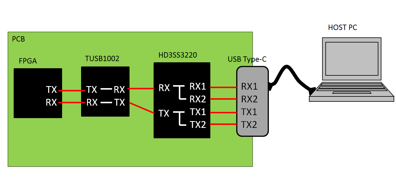
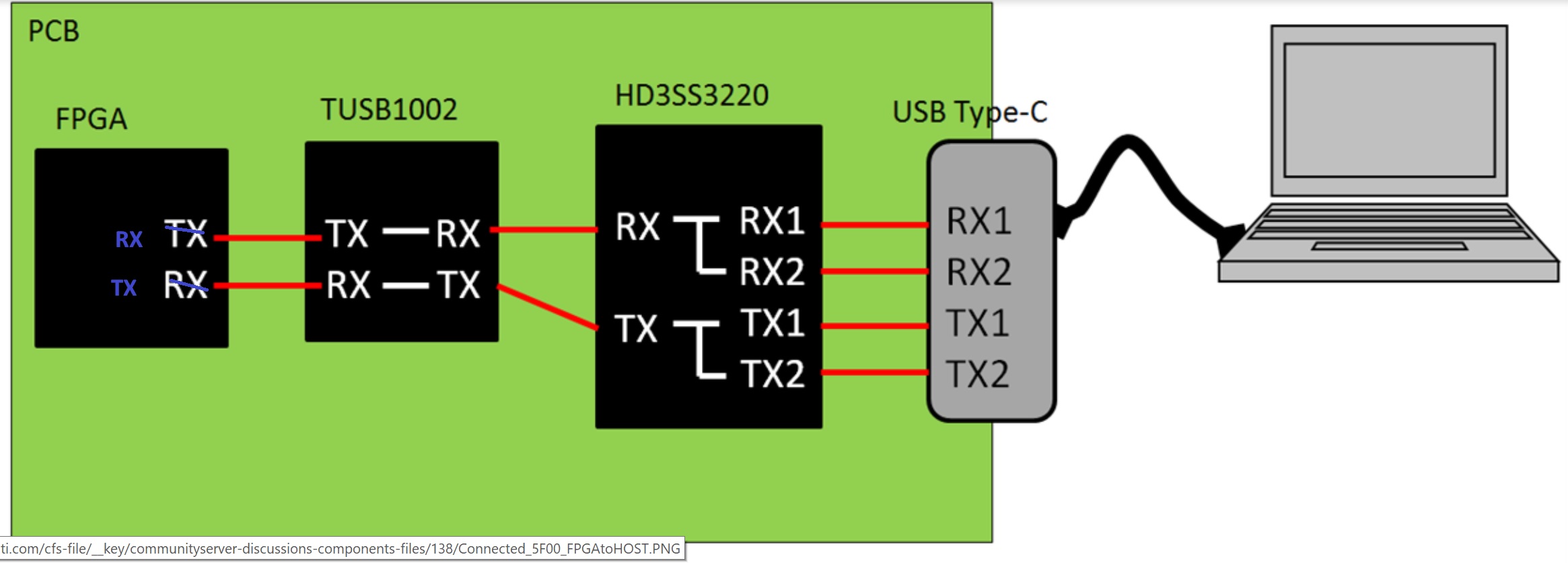
Could you check the schematic below? Customer wants to know if the connection is correct or not.
<Condition>
-USB2.0 is not used
-UFP only
/cfs-file/__key/communityserver-discussions-components-files/138/HD3SS3220-and-TUSB1002.pdf
<Questions from customer>
1. Is the connection of data bus between the TUSB1002 and HD3SS3220 correct by the combination of Rx and Tx?
2. The d/s states that the maximum resistance of VBUS_DET is 910kohm. If the resistance exceeds the 910kohm, what kind of problem would occur? Customer would like to use 910kohm in E24 series.
3. Are the CC1, 2 determined internal pull up or pull down by PORT-pin setting? Or does it require external pull down? Customer will use the device UFP only.
4. If the ENn_CC is disabled, where are the CC1 and CC2 pin set, Pull up? / Pull down? / Floating?
5. What happens if ENn_MUX is enabled and ENn_CC is disabled?
6. Since customer doesn't think to control this IC from the outside, customer is going to make 22, 24, 25 pins to NC. In the case of UFP, is there any problem without using I2C / GPIO?
7. Is the connection between the HD3SS3220 and the USB connector (Type-C) correct by the combination of Tx and Rx?
Regards,
Yamaguchi