Part Number: DS90C031
Other Parts Discussed in Thread: DS90C032,
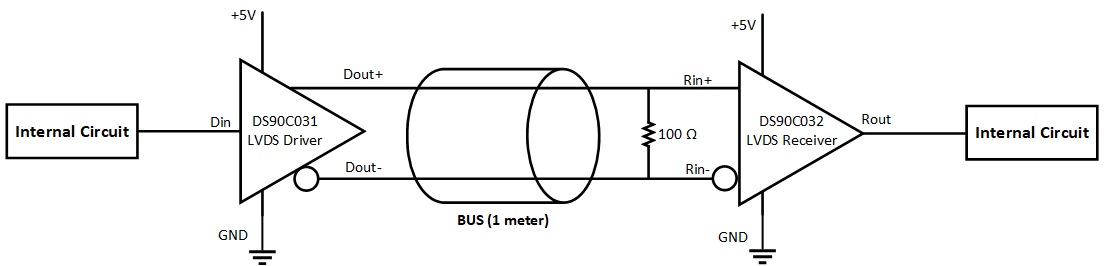
Devices used: DS90C031, DS90C032
1. When the input to the LVDS driver was fed with a 5V,500 KHz clock signal, the DOUT+ line at the LVDS driver ouptut was seen as stuck at 1.2 V. At the same time, the DOUT- line was showing normal LVDS output. Passive resistance measurements between DOUT+ to VDD (IC supply pin) showed 118 Ohm (after disconnecting from the bus and all devices powered OFF). What does this behaviour indicate? What could be the reason for this failure? What are the implications of this failure on the receiver device connected to the bus in such a scenario?
2. In a separate case, passive resistance measurements were carried out on separate LVDS receiver DS90C032 and driver DS90C031 ICs. However, the resistance values were found to be varying across different measurements (Multimeter used: Keysight U1252B multimeter). Can you please explain the reason for this observation?
3. For LVDS Receiver DS90C032 data sheet mentions pull up and pull down resistors at the inputs, but the values are not mentioned. Please provide the approximate values of on chip pull up and pull down resistors.
4. Is ESD protection circuitry available for all pins or specific pins?
5. How is the offset voltage of 1.2V maintained at LVDS driver output DOUT+ and DOUT-. Is it through resistive dividers or through active circuits?
6. If possible please provide a generic block diagram of LVDS driver and receiver ICs (DS90C031 and DS90C032)
Schematic drawing