Part Number: MAX3232
Hello TI.
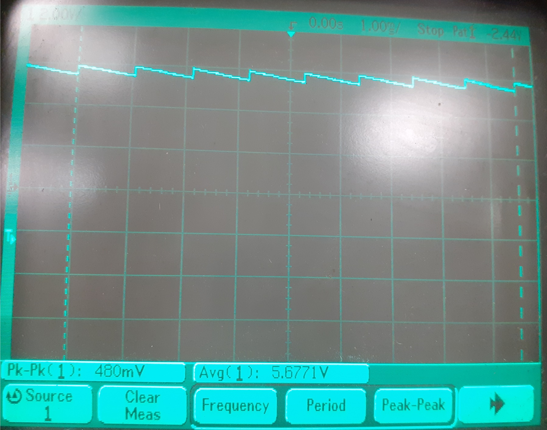
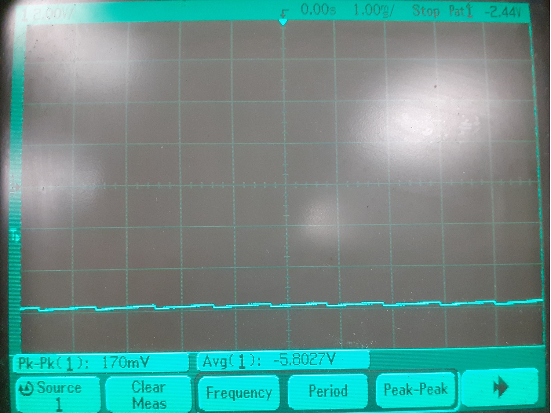
Figure 1 shows the output signal of the MAX3232 chip on the DOUT2 pin. Output DOUT1 has a clear signal. the range of the DOUT2 signal voltage is 480 mV, the amplitude is 5.67 V. Figure 2 shows the connection diagram of the MAX3232 chip with capacitors. Is there a solution to this problem?
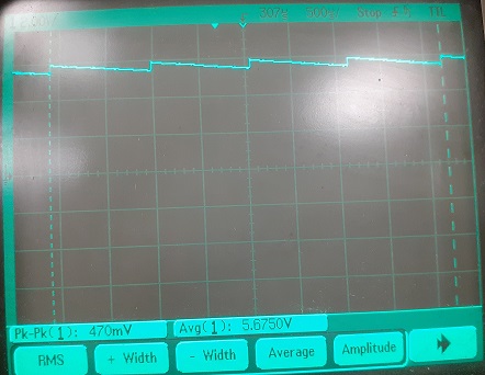
Figure 1
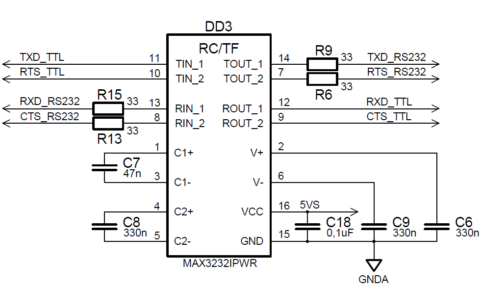
Figure 2
Best Regards, Vladimir.